

Philips BUK112-50GL Datasheet
Philips Semiconductors Product specification
PowerMOS transistor BUK112-50GL
Logic level TOPFET
DESCRIPTION QUICK REFERENCE DATA
Monolithic temperature and SYMBOL PARAMETER MAX. UNIT
overload protected logic level power
MOSFET in a 5 pin plastic V
envelope, intended as a low side I
switch for automotive applications. T
DS
D
j
R
DS(ON)
SYMBOL PARAMETER NOM. UNIT
Continuous drain source voltage 50 V
Continuous drain current 12 A
Continuous junction temperature 150 ˚C
Drain-source on-state resistance 93 mΩ
V
PS
Protection supply voltage 5 V
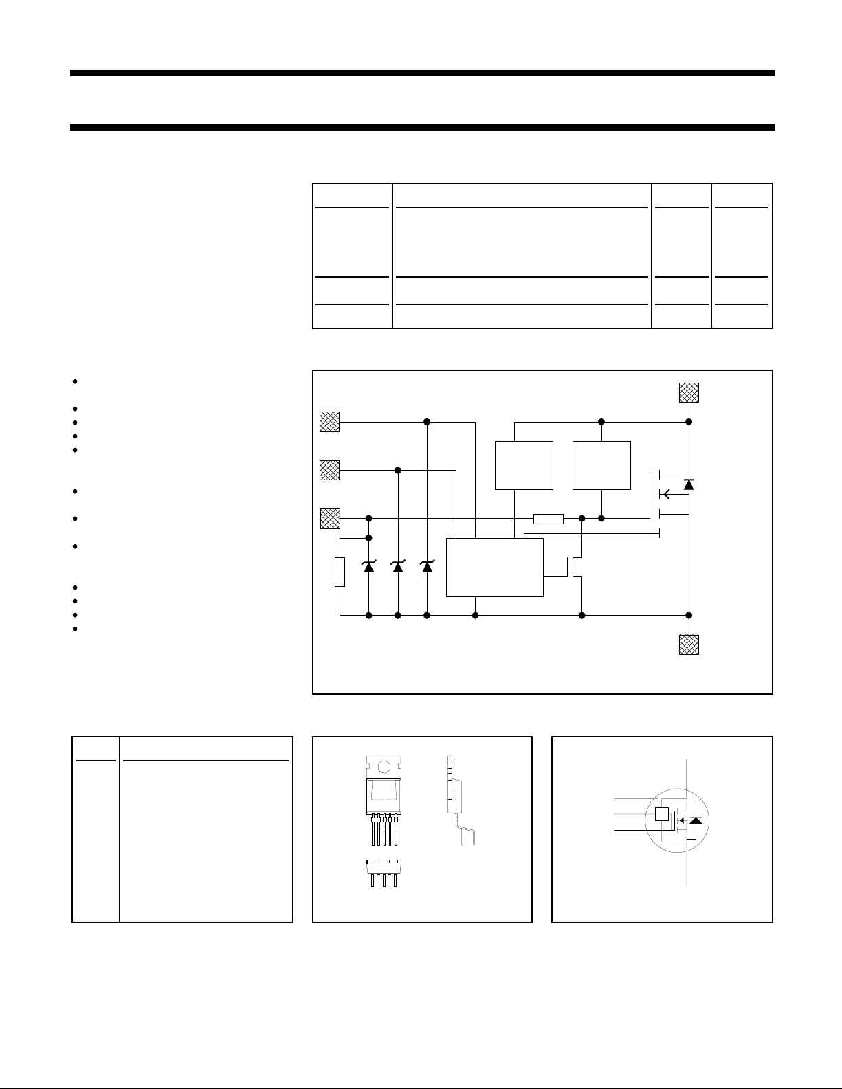
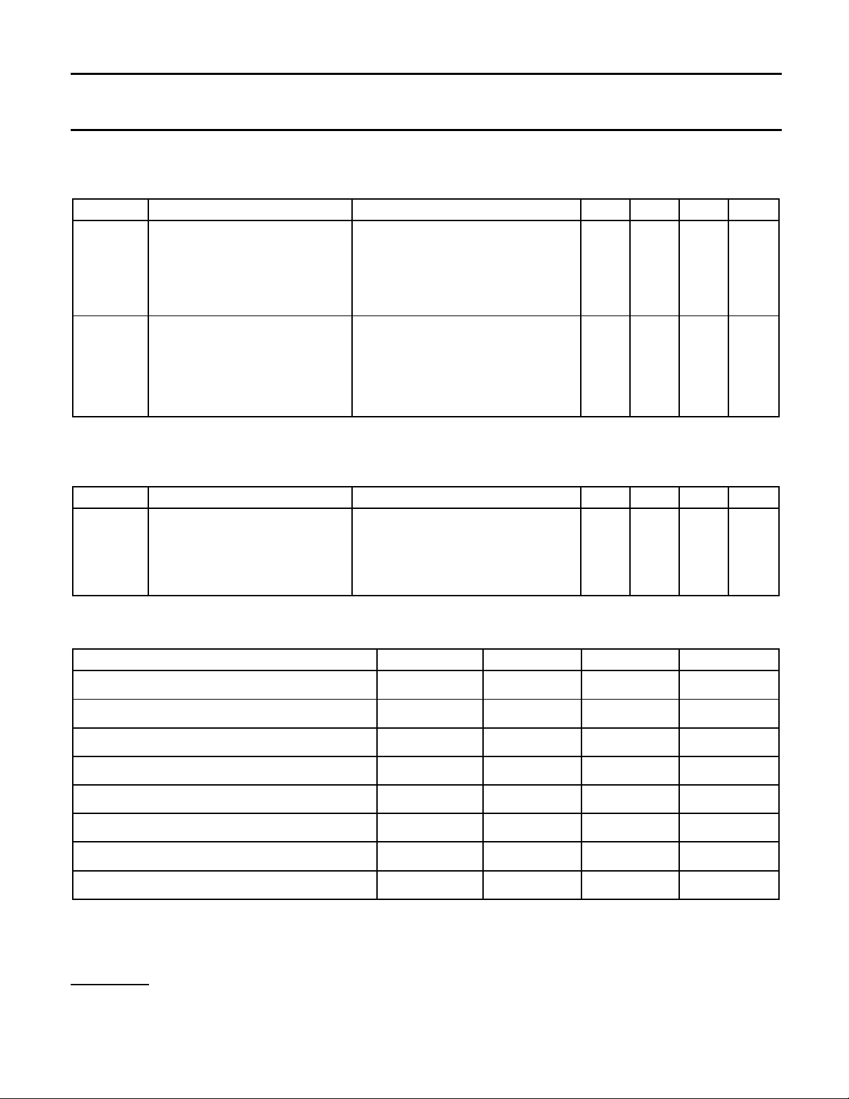
FEATURES FUNCTIONAL BLOCK DIAGRAM
Vertical power DMOS output
stage
Low on-state resistance
Low operating supply current
Overtemperature protection
Overload protection against
short circuit load with
drain current limiting
Latched overload protection
reset by protection supply
Protection circuit condition
indicated by flag pin
Off-state detection
of open circuit load
indicated by flag pin
5 V logic compatible input level
Integral input resistors.
ESD protection on all pins
Over voltage clamping
PROTECTION SUPPLY
FLAG
INPUT
RIS
Fig.1. Elements of the TOPFET.
OC LOAD
DETECT
RIG
LOGIC AND
PROTECTION
DRAIN
O/V
CLAMP
POWER
MOSFET
SOURCE
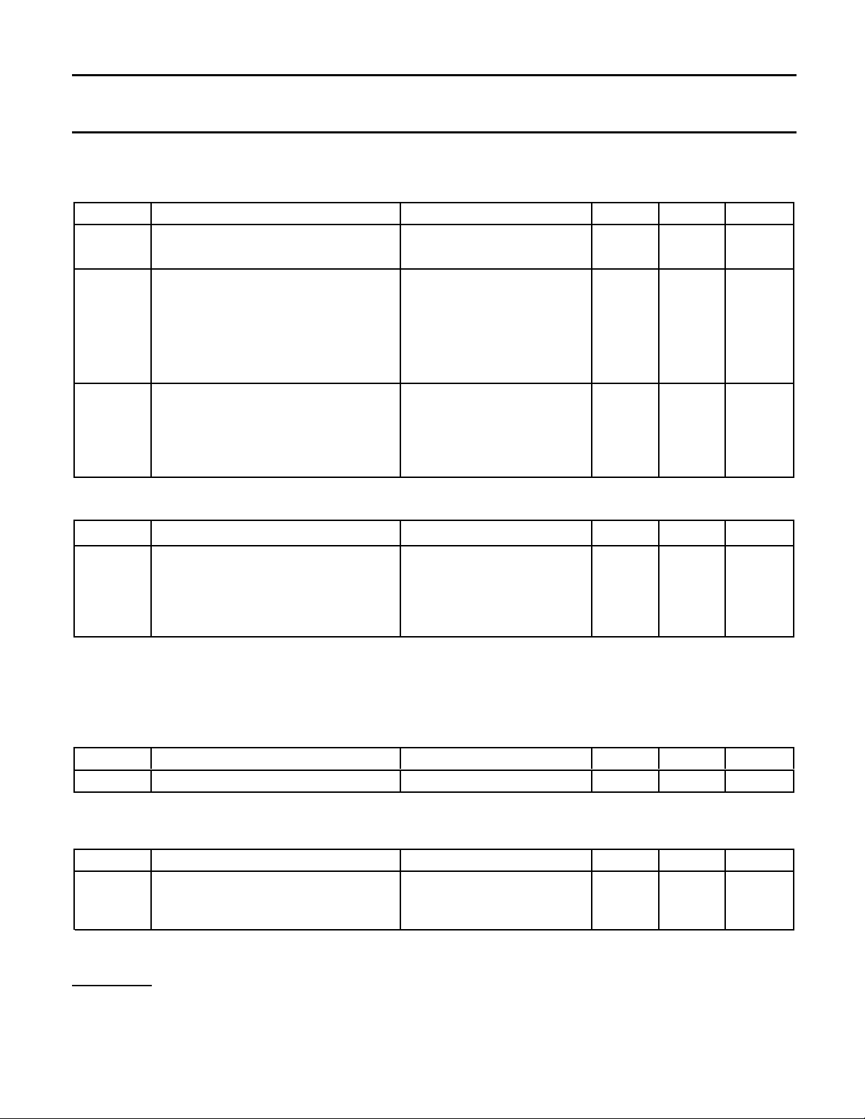
PINNING - SOT263 PIN CONFIGURATION SYMBOL
PIN DESCRIPTION
12345
tab
TOPFET
P
F
I
leadform
263-01
1 input
2 flag
3 drain
4 protection supply
5 source
Fig. 2. Fig. 3.
tab drain
September 1996 1 Rev 1.000
D
P
S
Philips Semiconductors Product specification
PowerMOS transistor BUK112-50GL
Logic level TOPFET
LIMITING VALUES
Limiting values in accordance with the Absolute Maximum Rating System (IEC 134)
SYMBOL PARAMETER CONDITIONS MIN. MAX. UNIT
Continuous voltage
V
DS
Drain source voltage
Continuous currents
I
D
I
I
I
F
I
P
Drain current VPS = 5 V; T
Input current - -5 5 mA
Flag current - -5 5 mA
Protection supply current - -5 5 mA
Thermal
P
tot
T
stg
T
j
T
sold
Total power dissipation Tmb = 25 ˚C - 52 W
Storage temperature - -55 175 ˚C
Junction temperature
Lead temperature during soldering - 260 ˚C
1
2
VIS = 0 V - 50 V
25 ˚C - self - A
VPS = 0 V; T
mb =
94 ˚C - 12 A
mb =
limited
continuous - 150 ˚C
ESD LIMITING VALUES
SYMBOL PARAMETER CONDITIONS MIN. MAX. UNIT
Electrostatic discharge capacitor Human body model;
voltages C = 100 pF; R = 1.5 kΩ
V
C1
V
C2
Drain to source - 4.5 kV
Input, flag or protection to source - 2 kV
OVERLOAD PROTECTION LIMITING VALUE
With the protection supply For overload conditions an n-MOS The drain current is limited to
connected, TOPFET can protect transistor turns on between the reduce dissipation in case of short
itself from two types of overload - gate and source to quickly circuit load. Refer to OVERLOAD
short circuit load and discharge the power MOSFET CHARACTERISTICS.
overtemperature. gate capacitance.
SYMBOL PARAMETER CONDITIONS MIN. MAX. UNIT
V
PSP
Protection supply voltage
3
for valid protection 4.5 - V
OVERVOLTAGE CLAMPING LIMITING VALUES
At a drain source voltage above 50 V the power MOSFET is actively turned on to clamp overvoltage transients.
SYMBOL PARAMETER CONDITIONS MIN. MAX. UNIT
E
DSM
E
DRM
Non-repetitive clamping energy IDM = 6 A; Tmb = 25˚C - 200 mJ
Repetitive clamping energy IDM = 3.1 A; VDD ≤ 20 V; - 20 mJ
Tmb ≤ 120˚C; f = 250 Hz
1 Prior to the onset of overvoltage clamping. For voltages above this value, safe operation is limited by the overvoltage clamping energy.
2 A higher Tj is allowed as an overload condition but at the threshold T
3 The minimum supply voltage required for correct operation of the overload protection circuits.
the over temperature trip operates to protect the switch.
j(TO)
September 1996 2 Rev 1.000
Philips Semiconductors Product specification
PowerMOS transistor BUK112-50GL
Logic level TOPFET
THERMAL CHARACTERISTICS
SYMBOL PARAMETER CONDITIONS MIN. TYP. MAX. UNIT
Thermal resistance
R
th j-mb
R
th j-a
OUTPUT CHARACTERISTICS
Tmb = 25 ˚C; VPS = 0 V unless otherwise specified
SYMBOL PARAMETER CONDITIONS MIN. TYP. MAX. UNIT
V
(CL)DSS
I
DSS
R
DS(ON)
Junction to mounting base - - - 2.38 K/W
Junction to ambient in free air - 60 - K/W
Off-state
Drain-source clamping voltage ID = 10 mA; -40˚C ≤ Tmb ≤ 150˚C 50 - 70 V
IDM = 0.75 A; tp ≤ 300 µs; δ ≤ 0.01 50 60 70 V
Drain-source leakage current1VIS = 0 V; VDS = 13 V - 0.5 10 µA
VDS = 50 V - 1 20 µA
Tmb = 125 ˚C; VDS = 40 V - 10 100 µA
On-state tp ≤ 300 µs; δ ≤ 0.01
Drain-source on-resistance IDM = 6 A; VIS = 4.4 V; VPS = 4.5 V - 70 93 mΩ
Tmb = 150 ˚C - 135 165 mΩ
INPUT CHARACTERISTICS
Tmb = 25 ˚C unless otherwise specified
SYMBOL PARAMETER CONDITIONS MIN. TYP. MAX. UNIT
Normal operation
V
I
IS
V
R
IS(TO)
(CL)IS
IG
Input threshold voltage VDS = 13 V; VPS = 0 V; ID = 1 mA 1 1.5 2 V
-40˚C ≤ Tmb ≤ 150˚C 0.5 - 2.5 V
Input current VIS = 5 V -40˚C ≤ Tmb ≤ 150˚C 200 350 500 µA
Input clamping voltage II = 1.5 mA 6 7.1 - V
Internal series resistance to gate of power MOSFET - 1.5 - kΩ
Overload protection latched
I
ISL
Input current VPS = 5 V; VIS = 5 V 1.5 3.2 4 mA
REVERSE CHARACTERISTICS
Tmb = 25 ˚C
SYMBOL PARAMETER CONDITIONS MIN. TYP. MAX. UNIT
-V
-V
-V
-V
DS
IS
PS
FS
Reverse drain voltage
Reverse input voltage -II = 5 mA - 0.7 - V
Reverse protection pin voltage -IP = 5 mA - 0.7 - V
Reverse flag voltage -IF = 5 mA - 0.7 - V
2
-ID = 6 A - 0.8 - V
1 The drain current required for open circuit load detection is switched off when there is no protection supply, in order to ensure a low off-state
2 Protection functions are disabled during reverse conduction.
quiescent current. Refer to OPEN CIRCUIT LOAD DETECTION CHARACTERISTICS.
September 1996 3 Rev 1.000
Philips Semiconductors Product specification
PowerMOS transistor BUK112-50GL
Logic level TOPFET
PROTECTION SUPPLY CHARACTERISTICS
Tmb = 25 ˚C unless otherwise specified
SYMBOL PARAMETER CONDITIONS MIN. TYP. MAX. UNIT
Normal operation or
protection latched
IPS, I
V
(CL)PS
PSL
Supply current VPS = 4.5 V - 330 400 µA
-40˚C ≤ Tmb ≤ 150˚C - - 450 µA
Clamping voltage IP = 1.5 mA 6 7.1 - V
Overload protection latched
V
PSR
Reset voltage - 2.1 - V
-40˚C ≤ Tmb ≤ 150˚C 1.5 - 3 V
t
pr
Reset time VPS = 0 V - 25 - µs
-40˚C ≤ Tmb ≤ 150˚C - - 150 µs
OPEN CIRCUIT LOAD DETECTION CHARACTERISTICS
An open circuit load condition can be detected while the TOPFET is in the off-state.
-40˚C ≤ Tmb ≤ 150˚C; VPS = 5 V; VDS = 13 V unless otherwise specified
SYMBOL PARAMETER CONDITIONS MIN. TYP. MAX. UNIT
I
I
V
DSP
DSF
ISF
Off-state drain current
Off-state drain threshold current VIS = 0 V; IF = 100 µA 0.4 1.1 - mA
Input threshold voltage
1
2
VIS = 0 V 0.5 1.4 2 mA
IF = 100 µA; ID = 100 µA; - 1.2 - V
Tmb = 25 ˚C
TRUTH TABLE
For normal, open-circuit load and overload conditions or inadequate protection supply voltage.
CONDITION PROTECTION INPUT FLAG OUTPUT
Normal on-state 1 1 0 1
Normal off-state 1 0 0 0
Open circuit load 1 1 0 1
Open circuit load 1 0 1 0
Short circuit load 1 1 1 0
Over temperature 1 X 1 0
Low protection supply voltage 0 1 1 1
Low protection supply voltage 0 0 1 0
For protection ‘0’ equals low, ‘1’ equals high.
For input ‘0’ equals low, ‘1’ equals high, ‘X’ equals don’t care.
For flag ‘0’ equals low, ‘1’ equals open or high.
For output switch ‘0’ equals off, ‘1’ equals on.
1 The drain source current which flows when the protection supply is high and the input is low.
2 For open circuit load indication, VIS must be less than V
.
ISF
September 1996 4 Rev 1.000

Philips Semiconductors Product specification
PowerMOS transistor BUK112-50GL
Logic level TOPFET
OVERLOAD CHARACTERISTICS
Tmb = 25 ˚C; VPS = 5 V unless otherwise specified
SYMBOL PARAMETER CONDITIONS MIN. TYP. MAX. UNIT
Short circuit load protection VIS = 5 V
I
D
P
D(TO)
E
DSC
I
DM
T
j(TO)
FLAG CHARACTERISTICS
The flag is an open drain transistor which requires an external pull-up circuit.
Tmb = 25 ˚C unless otherwise specified
SYMBOL PARAMETER CONDITIONS MIN. TYP. MAX. UNIT
V
FSF
I
FSF
I
FSO
V
(CL)FS
V
PSF
R
F
Drain current limiting VDS = 13 V -40˚C ≤ Tmb ≤ 150˚C 12 24 36 A
Overload power threshold
Characteristic energy which determines trip time
Peak drain current
3
1
for protection to operate - 100 - W
2
- 200 - mJ
VDD = 13 V; RL ≤ 10 mΩ -45- A
Overtemperature protection
Threshold temperature ID ≥ 1 A 150 185 215 ˚C
Flag ‘low’ normal operation; VPS = 5 V
Flag voltage IF = 100 µA - 0.7 - V
-40˚C ≤ Tmb ≤ 150˚C - - 0.9 V
Flag saturation current VFS = 5 V - 10 - mA
Flag ‘high’ overload or fault
Flag leakage current VFS = 5 V - 0.1 1 µA
Tmb = 150˚C - 1 10 µA
Flag clamping voltage IF = 100 µA 6 6.9 - V
Protection supply threshold IF = 100 µA; VDS = 5 V 2.5 3 4 V
voltage
4
-40˚C ≤ Tmb ≤ 150˚C 2 - 4 V
Application information
Suitable external pull-up VFF = 5 V - 50 - kΩ
resistance
1 Refer to figure 15.
2 Trip time t
3 For short circuit load connected after turn-on.
4 When VPS is less than V
d sc
≈ E
/ [ PD - P
DSC
]. Refer also to figure 15.
D(TO)
the flag pin indicates low protection supply voltage. Refer to TRUTH TABLE.
PSF
September 1996 5 Rev 1.000
 Loading...