

Philips BUK107-50GL Datasheet
Philips Semiconductors Product specification
PowerMOS transistor BUK107-50GL
Logic level TOPFET
DESCRIPTION QUICK REFERENCE DATA
Monolithic overload protected logic SYMBOL PARAMETER MAX. UNIT
level power MOSFET in a surface
mount plastic envelope, intended as V
DS
Continuous drain source voltage 50 V
a general purpose switch for
automotive systems and other I
D
Continuous drain current 0.5 A
applications.
P
D
Total power dissipation 1.8 W
APPLICATIONS
T
j
Continuous junction temperature 150 ˚C
General controller for driving
lamps R
DS(ON)
Drain-source on-state resistance 200 mΩ
small motors
solenoids
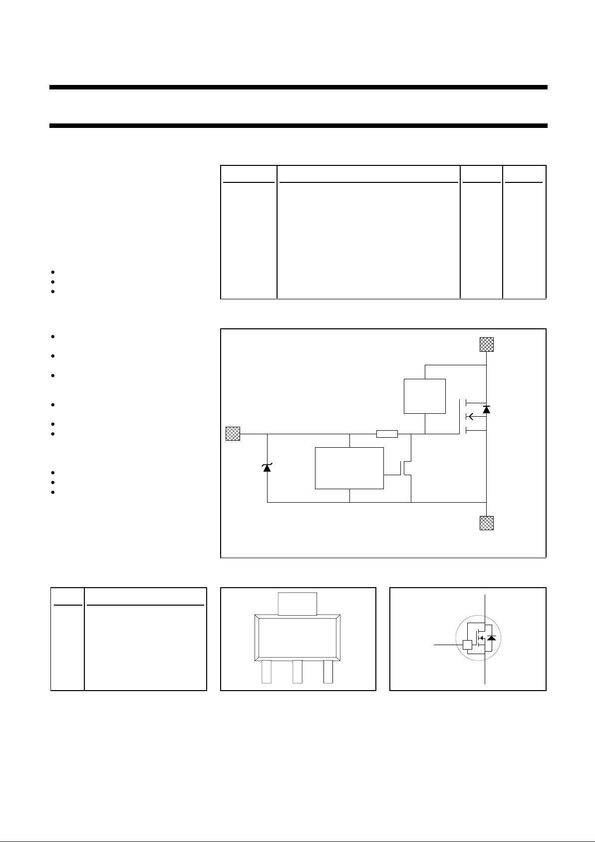
FEATURES FUNCTIONAL BLOCK DIAGRAM
Vertical power DMOS output
stage
Overload protected up to
85˚C ambient
Overload protection by current
limiting and overtemperature
sensing
Latched overload protection
reset by input
5 V logic compatible input level
Control of power MOSFET
and supply of overload
protection circuits
derived from input
Low operating input current
ESD protection on all pins
Overvoltage clamping for turn
off of inductive loads
Fig.1. Elements of the TOPFET.
PINNING - SOT223 PIN CONFIGURATION SYMBOL
PIN DESCRIPTION
1 input
2 drain
3 source
4 drain (tab)
POWER
MOSFET
DRAIN
SOURCE
INPUT
O/V
CLAMP
LOGIC AND
PROTECTION
RIG
4
1
23
P
D
S
I
TOPFET
April 1998 1 Rev 1.200
Philips Semiconductors Product specification
PowerMOS transistor BUK107-50GL
Logic level TOPFET
LIMITING VALUES
Limiting values in accordance with the Absolute Maximum System (IEC 134)
SYMBOL PARAMETER CONDITIONS MIN. MAX. UNIT
V
DS
Continuous drain source voltage
1
- - 50 V
I
D
Continuous drain current
2
- - self limiting A
I
I
Continuous input current clamping - 3 mA
I
IRM
Non-repetitive peak input current tp ≤ 1 ms - 10 mA
P
D
Total power dissipation T
amb
= 25 ˚C - 1.8 W
T
stg
Storage temperature - -55 150 ˚C
T
j
Continuous junction temperature normal operation
3
- 150 ˚C
ESD LIMITING VALUE
SYMBOL PARAMETER CONDITIONS MIN. MAX. UNIT
V
C
Electrostatic discharge capacitor Human body model; - 2 kV
voltage C = 250 pF; R = 1.5 kΩ
OVERVOLTAGE CLAMPING LIMITING VALUES
At a drain source voltage above 50 V the power MOSFET is actively turned on to clamp overvoltage transients.
SYMBOL PARAMETER CONDITIONS MIN. MAX. UNIT
E
DSM
Non-repetitive clamping energy Tb ≤ 25 ˚C; IDM < I
D(lim)
; - 100 mJ
inductive load
E
DRM
Repetitive clamping energy Tb ≤ 75 ˚C; IDM = 50 mA; - 4 mJ
f = 250 Hz
OVERLOAD PROTECTION LIMITING VALUES
With the protection supply provided via the input pin, TOPFET can protect itself from short circuit loads.
Overload protection operates by means of drain current limiting and activating the overtemperature protection.
SYMBOL PARAMETER CONDITIONS MIN. MAX. UNIT
V
DDP
Protected drain source supply voltage VIS = 5 V - 35 V
VIS = 4 V - 16 V
OVERLOAD PROTECTION CHARACTERISTICS
TOPFET switches off to protect itself when there is an overload fault condition.
It remains latched off until reset by the input.
SYMBOL PARAMETER CONDITIONS MIN. TYP. MAX. UNIT
Overload protection
I
D(lim)
Drain current limiting VIS = 5 V 0.5 1.1 1.5 A
Overtemperature protection only in drain current limiting
T
j(TO)
Threshold junction temperature VIS = 5 V 100 130 160 ˚C
1 Prior to the onset of overvoltage clamping. For voltages above this value, safe operation is limited by the overvoltage clamping energy.
2 Refer to OVERLOAD PROTECTION CHARACTERISTICS.
3 Not in an overload condition with drain current limiting.
April 1998 2 Rev 1.200

Philips Semiconductors Product specification
PowerMOS transistor BUK107-50GL
Logic level TOPFET
THERMAL CHARACTERISTICS
SYMBOL PARAMETER CONDITIONS MIN. TYP. MAX. UNIT
Thermal resistance
R
th j-sp
Junction to solder point - 12 18 K/W
R
th j-b
Junction to board
1
Mounted on any PCB - 40 - K/W
R
th j-a
Junction to ambient Mounted on PCB of fig. 19 - - 70 K/W
STATIC CHARACTERISTICS
Tb = 25 ˚C unless otherwise specified
SYMBOL PARAMETER CONDITIONS MIN. TYP. MAX. UNIT
V
(CL)DSS
Drain-source clamping voltage VIS = 0 V; ID = 10 mA 50 55 - V
V
(CL)DSS
Drain-source clamping voltage VIS = 0 V; IDM = 200 mA; - 56 70 V
tp ≤ 300 µs; δ ≤ 0.01
I
DSS
Off-state drain current VDS = 45 V; VIS = 0 V - 0.5 2 µA
I
DSS
Off-state drain current VDS = 50 V; VIS = 0 V - 1 20 µA
I
DSS
Off-state drain current VDS = 40 V; VIS = 0 V; Tj = 100 ˚C - 10 100 µA
R
DS(ON)
Drain-source on-state VIS = 5 V; IDM = 100 mA; - 150 200 mΩ
resistance tp ≤ 300 µs; δ ≤ 0.01
INPUT CHARACTERISTICS
Tb = 25 ˚C unless otherwise specified. The supply for the logic and overload protection is taken from the input.
SYMBOL PARAMETER CONDITIONS MIN. TYP. MAX. UNIT
V
IS(TO)
Input threshold voltage VDS = 5 V; ID = 1 mA 1.7 2.2 2.7 V
I
IS
Input supply current normal operation; VIS = 5 V - 330 450 µA
VIS = 4 V - 170 270 µA
I
ISL
Input supply current protection latched; VIS = 5 V - 1.45 2 mA
VIS = 3.5 V - 0.95 1.3 mA
V
ISR
Protection latch reset voltage
2
1 2.7 3.5 V
V
(CL)IS
Input clamping voltage II = 1.5 mA 6 7.5 - V
R
IG
Input series resistance to gate of power MOSFET - 4.5 - kΩ
1 Temperature measured 1.3 mm from tab.
2 The input voltage below which the overload protection circuits will be reset.
April 1998 3 Rev 1.200
 Loading...