

Philips BUK100-50GL Datasheet
Philips Semiconductors Product specification
PowerMOS transistor BUK100-50GL
Logic level TOPFET
DESCRIPTION QUICK REFERENCE DATA
Monolithic temperature and SYMBOL PARAMETER MAX. UNIT
overload protected logic level power
MOSFET in a 3 pin plastic V
envelope, intended as a general I
purpose switch for automotive P
systems and other applications. T
D
R
DS
D
j
DS(ON)
APPLICATIONS V
General controller for driving
lamps
motors
solenoids
heaters
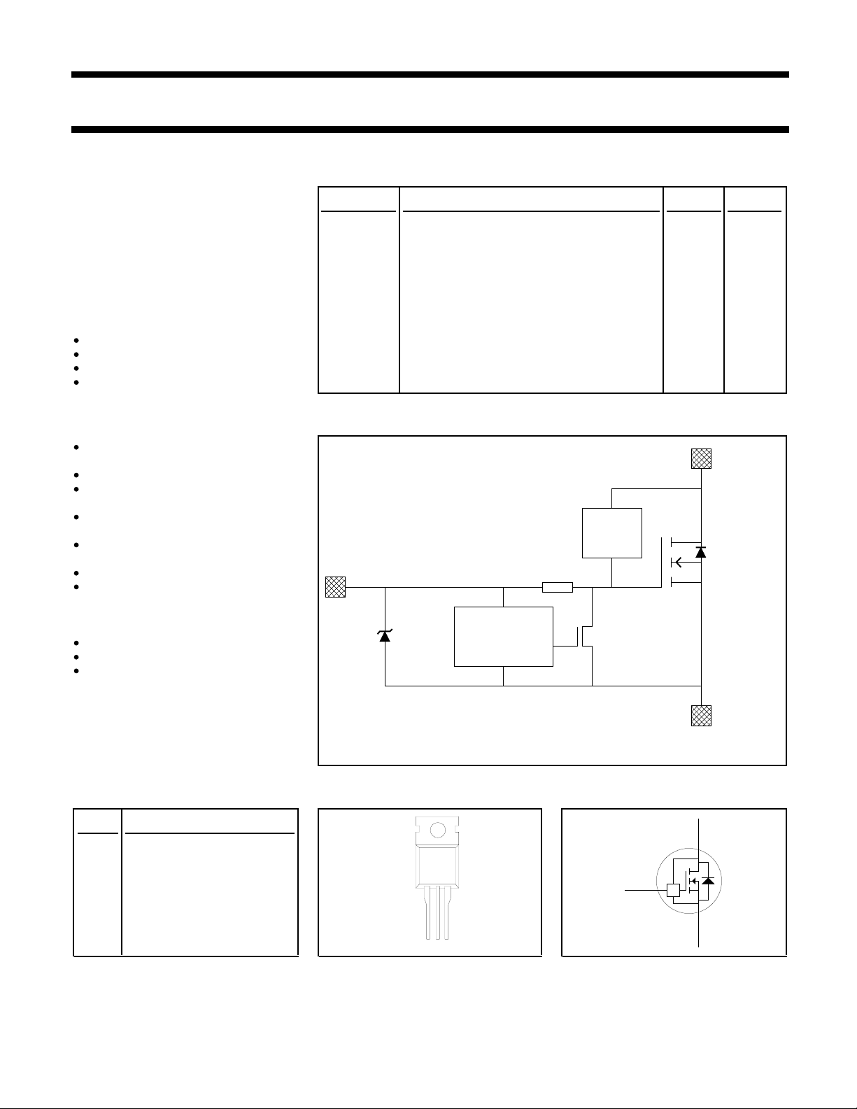
FEATURES FUNCTIONAL BLOCK DIAGRAM
Vertical power DMOS output
stage
Low on-state resistance
Overload protection against
over temperature
Overload protection against
short circuit load
Latched overload protection
reset by input
5 V logic compatible input level
Control of power MOSFET
and supply of overload
protection circuits
derived from input
Low operating input current
ESD protection on input pin
Overvoltage clamping for turn
off of inductive loads
INPUT
Continuous drain source voltage 50 V
Continuous drain current 13.5 A
Total power dissipation 40 W
Continuous junction temperature 150 ˚C
Drain-source on-state resistance 125 mΩ
= 5 V
IS
DRAIN
O/V
CLAMP
RIG
LOGIC AND
PROTECTION
POWER
MOSFET
SOURCE
Fig.1. Elements of the TOPFET.
PINNING - TO220AB PIN CONFIGURATION SYMBOL
PIN DESCRIPTION
1 input
2 drain
tab
TOPFET
I
3 source
tab drain
123
November 1996 1 Rev 1.300
D
P
S

Philips Semiconductors Product specification
PowerMOS transistor BUK100-50GL
Logic level TOPFET
LIMITING VALUES
Limiting values in accordance with the Absolute Maximum Rating System (IEC 134)
SYMBOL PARAMETER CONDITIONS MIN. MAX. UNIT
V
V
I
D
I
D
I
DRM
P
T
T
T
DSS
IS
D
stg
j
sold
Continuous off-state drain source VIS = 0 V - 50 V
voltage
1
Continuous input voltage - 0 6 V
Continuous drain current T
Continuous drain current T
25 ˚C; VIS = 5 V - 13.5 A
mb ≤
100 ˚C; VIS = 5 V - 8.5 A
mb ≤
Repetitive peak on-state drain current Tmb ≤ 25 ˚C; VIS = 5 V - 54 A
Total power dissipation Tmb ≤ 25 ˚C - 40 W
Storage temperature - -55 150 ˚C
Continuous junction temperature
2
normal operation - 150 ˚C
Lead temperature during soldering - 250 ˚C
OVERLOAD PROTECTION LIMITING VALUES
With the protection supply provided via the input pin, TOPFET can protect itself from two types of overload.
SYMBOL PARAMETER CONDITIONS MIN. MAX. UNIT
V
V
V
P
ISP
DDP(T)
DDP(P)
DSM
Protection supply voltage
Over temperature protection
Protected drain source supply voltage VIS = 5 V - 50 V
Short circuit load protection
Protected drain source supply voltage4VIS = 5 V - 35 V
Instantaneous overload dissipation Tmb = 25 ˚C - 0.6 kW
3
for valid protection 4 - V
OVERVOLTAGE CLAMPING LIMITING VALUES
At a drain source voltage above 50 V the power MOSFET is actively turned on to clamp overvoltage transients.
SYMBOL PARAMETER CONDITIONS MIN. MAX. UNIT
I
DROM
E
DSM
Repetitive peak clamping current VIS = 0 V - 15 A
Non-repetitive clamping energy Tmb ≤ 25 ˚C; IDM = 15 A; - 200 mJ
VDD ≤ 20 V; inductive load
E
DRM
Repetitive clamping energy Tmb ≤ 95 ˚C; IDM = 4 A; - 20 mJ
VDD ≤ 20 V; f = 250 Hz
ESD LIMITING VALUE
SYMBOL PARAMETER CONDITIONS MIN. MAX. UNIT
V
C
1 Prior to the onset of overvoltage clamping. For voltages above this value, safe operation is limited by the overvoltage clamping energy.
2 A higher Tj is allowed as an overload condition but at the threshold T
3 The input voltage for which the overload protection circuits are functional.
4 The device is able to self-protect against a short circuit load providing the drain-source supply voltage does not exceed V
Electrostatic discharge capacitor Human body model; - 2 kV
voltage C = 250 pF; R = 1.5 kΩ
the over temperature trip operates to protect the switch.
j(TO)
For further information, refer to OVERLOAD PROTECTION CHARACTERISTICS.
DDP(P)
maximum.
November 1996 2 Rev 1.300

Philips Semiconductors Product specification
PowerMOS transistor BUK100-50GL
Logic level TOPFET
THERMAL CHARACTERISTICS
SYMBOL PARAMETER CONDITIONS MIN. TYP. MAX. UNIT
Thermal resistance
R
R
th j-mb
th j-a
Junction to mounting base - - 2.5 3.1 K/W
Junction to ambient in free air - 60 - K/W
STATIC CHARACTERISTICS
Tmb = 25 ˚C unless otherwise specified
SYMBOL PARAMETER CONDITIONS MIN. TYP. MAX. UNIT
V
(CL)DSS
V
(CL)DSS
Drain-source clamping voltage VIS = 0 V; ID = 10 mA 50 - - V
Drain-source clamping voltage VIS = 0 V; IDM = 1 A; tp ≤ 300 µs; - - 70 V
δ ≤ 0.01
I
I
I
R
DSS
DSS
DSS
DS(ON)
Zero input voltage drain current VDS = 12 V; VIS = 0 V - 0.5 10 µA
Zero input voltage drain current VDS = 50 V; VIS = 0 V - 1 20 µA
Zero input voltage drain current VDS = 40 V; VIS = 0 V; Tj = 125 ˚C - 10 100 µA
Drain-source on-state VIS = 5 V; IDM = 7.5 A; tp ≤ 300 µs; - 85 125 mΩ
resistance δ ≤ 0.01
OVERLOAD PROTECTION CHARACTERISTICS
TOPFET switches off when one of the overload thresholds is reached. It remains latched off until reset by the input.
SYMBOL PARAMETER CONDITIONS MIN. TYP. MAX. UNIT
E
t
T
d sc
DS(TO)
j(TO)
Short circuit load protection1Tmb = 25 ˚C; L ≤ 10 µH
Overload threshold energy VDD = 13 V; VIS = 5 V - 0.2 - J
Response time VDD = 13 V; VIS = 5 V - 0.8 - ms
Over temperature protection
Threshold junction temperature VIS = 5 V; from ID ≥ 1 A
2
150 - - ˚C
INPUT CHARACTERISTICS
Tmb = 25 ˚C unless otherwise specified. The supply for the logic and overload protection is taken from the input.
SYMBOL PARAMETER CONDITIONS MIN. TYP. MAX. UNIT
V
IS(TO)
I
IS
V
ISR
V
ISR
I
ISL
V
(BR)IS
R
IG
1 The short circuit load protection is able to save the device providing the instantaneous on-state dissipation is less than the limiting value for
2 The over temperature protection feature requires a minimum on-state drain source voltage for correct operation. The specified minimum I
3 The input voltage below which the overload protection circuits will be reset.
November 1996 3 Rev 1.300
Input threshold voltage VDS = 5 V; ID = 1 mA 1.0 1.5 2.0 V
Input supply current VIS = 5 V; normal operation - 0.2 0.35 mA
Protection reset voltage
3
2.0 2.6 3.5 V
Protection reset voltage Tj = 150 ˚C 1.0 - Input supply current VIS = 5 V; protection latched 0.5 1.2 2.0 mA
Input clamp voltage II = 10 mA 6 - - V
Input series resistance to gate of power MOSFET - 4 - kΩ
P
, which is always the case when VDS is less than V
DSM
ensures this condition.
maximum. Refer to OVERLOAD PROTECTION LIMITING VALUES.
DSP
D
Philips Semiconductors Product specification
PowerMOS transistor BUK100-50GL
Logic level TOPFET
TRANSFER CHARACTERISTICS
Tmb = 25 ˚C
SYMBOL PARAMETER CONDITIONS MIN. TYP. MAX. UNIT
g
fs
I
D(SC)
SWITCHING CHARACTERISTICS
Tmb = 25 ˚C. RI = 50 Ω . Refer to waveform figures and test circuits.
SYMBOL PARAMETER CONDITIONS MIN. TYP. MAX. UNIT
Forward transconductance VDS = 10 V; IDM = 7.5 A tp ≤ 300 µs; 5 9 - S
δ ≤ 0.01
Drain current
1
VDS = 13 V; VIS = 5 V - 25 - A
t
d on
t
r
t
d off
t
f
t
d on
t
r
t
d off
t
f
Turn-on delay time VDD = 13 V; VIS = 5 V - 1.5 - µs
Rise time resistive load RL = 4 Ω -8-µs
Turn-off delay time VDD = 13 V; VIS = 0 V - 6 - µs
Fall time resistive load RL = 4 Ω - 4.5 - µs
Turn-on delay time VDD = 13 V; VIS = 5 V - 1.5 - µs
Rise time inductive load IDM = 3 A - 1 - µs
Turn-off delay time VDD = 13 V; VIS = 0 V - 10 - µs
Fall time inductive load IDM = 3 A - 0.5 - µs
REVERSE DIODE LIMITING VALUE
SYMBOL PARAMETER CONDITIONS MIN. MAX. UNIT
I
S
Continuous forward current Tmb ≤ 25 ˚C; VIS = 0 V - 13.5 A
REVERSE DIODE CHARACTERISTICS
Tmb = 25 ˚C
SYMBOL PARAMETER CONDITIONS MIN. TYP. MAX. UNIT
V
SDS
t
rr
Forward voltage IS = 15 A; VIS = 0 V; tp = 300 µs - 1.0 1.5 V
Reverse recovery time not applicable
2
----
ENVELOPE CHARACTERISTICS
SYMBOL PARAMETER CONDITIONS MIN. TYP. MAX. UNIT
L
d
L
d
L
s
1 During overload before short circuit load protection operates.
2 The reverse diode of this type is not intended for applications requiring fast reverse recovery.
November 1996 4 Rev 1.300
Internal drain inductance Measured from contact screw on - 3.5 - nH
tab to centre of die
Internal drain inductance Measured from drain lead 6 mm - 4.5 - nH
from package to centre of die
Internal source inductance Measured from source lead 6 mm - 7.5 - nH
from package to source bond pad
 Loading...