

Philips BUJ205A Datasheet
Philips Semiconductors Objective specification
Silicon Diffused Power Transistor BUJ205A
GENERAL DESCRIPTION
High-voltage, high-speed planar-passivated npn power switching transistor in TO220AB envelope intended for use
in high frequency electronic lighting ballast applications, converters, inverters, switching regulators, motor control
systems, etc.
QUICK REFERENCE DATA
SYMBOL PARAMETER CONDITIONS TYP. MAX. UNIT
V
CESM
V
CBO
V
CEO
I
C
I
CM
P
tot
V
CEsat
t
f
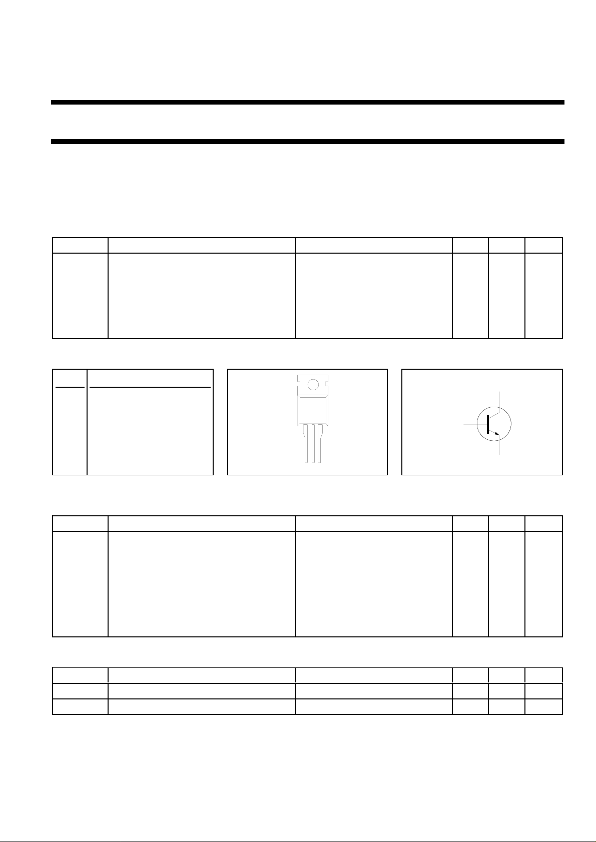
PINNING - TO220AB PIN CONFIGURATION SYMBOL
Collector-emitter voltage peak value VBE = 0 V - 850 V
Collector-Base voltage (open emitter) - 850 V
Collector-emitter voltage (open base) - 450 V
Collector current (DC) - 8 A
Collector current peak value - 12 A
Total power dissipation Tmb ≤ 25 ˚C - 125 W
Collector-emitter saturation voltage IC = 5.0 A;IB = 1.0 A - 1.5 V
Fall time Ic=6A,IB1=1.2A - 300 µs
PIN DESCRIPTION
tab
c
1 base
2 collector
b
3 emitter
tab collector
123
LIMITING VALUES
Limiting values in accordance with the Absolute Maximum Rating System (IEC 134)
SYMBOL PARAMETER CONDITIONS MIN. MAX. UNIT
V
V
V
I
C
I
CM
I
B
I
BM
P
T
T
CESM
CEO
CBO
tot
stg
j
Collector to emitter voltage VBE = 0 V - 850 V
Collector to emitter voltage (open base) - 450 V
Collector to base voltage (open emitter) - 850 V
Collector current (DC) - 8 A
Collector current peak value - 12 A
Base current (DC) - 4 A
Base current peak value - 6 A
Total power dissipation Tmb ≤ 25 ˚C - 125 W
Storage temperature -65 150 ˚C
Junction temperature - 150 ˚C
THERMAL RESISTANCES
e
SYMBOL PARAMETER CONDITIONS TYP. MAX. UNIT
R
R
th j-mb
th j-a
Junction to mounting base - 1 K/W
Junction to ambient in free air 60 - K/W
August 1998 1 Rev 1.000

Philips Semiconductors Objective specification
Silicon Diffused Power Transistor BUJ205A
STATIC CHARACTERISTICS
Tmb = 25 ˚C unless otherwise specified
SYMBOL PARAMETER CONDITIONS MIN. TYP. MAX. UNIT
I
CES
I
CES
I
EBO
V
CEOsust
V
CEsat
V
BEsat
h
FE
Collector cut-off current
Emitter cut-off current VEB = 9 V; IC = 0 A - - 10 mA
Collector-emitter sustaining voltage IB = 0 A; IC = 100 mA; 450 - - V
Collector-emitter saturation voltage IC = 5 A; IB = 1.0 A - - 1.5 V
Base-emitter saturation voltage IC = 6 A; IB = 1.2 A - - 1.5 V
DC current gain IC = 10 mA; VCE = 5 V 10 - 35
DYNAMIC CHARACTERISTICS
Tmb = 25 ˚C unless otherwise specified
SYMBOL PARAMETER CONDITIONS TYP. MAX. UNIT
Switching times (resistive load) I
t
on
t
s
t
f
t
s
t
f
t
s
t
f
Turn-on time - 1.0 µs
Turn-off storage time - 4 µs
Turn-off fall time - 0.8 µs
Switching times (inductive load) I
Turn-off storage time - 1.5 µs
Turn-off fall time - 300 ns
Switching times (inductive load) I
Turn-off storage time - 2.5 µs
Turn-off fall time - 300 ns
1
VBE = 0 V; VCE = V
VBE = 0 V; VCE = V
Tj = 125 ˚C
CESMmax
;--3mA
CESMmax
--1mA
L = 25 mH
IC = 1.0A; VCE = 5 V 10 - 35
= 6.0 A; I
Con
RL = 75 ohms; V
= 6.0 A; I
Con
-VBB = 5 V
= 6.0 A; I
Con
= -I
Bon
Bon
Bon
= 1.2 A;
Boff
= 4 V;
BB2
= 1.2 A; LB = 1 µH;
= 1.2 A; LB = 1 µH;
-VBB = 5 V; Tj = 100 ˚C
1 Measured with half sine-wave voltage (curve tracer).
August 1998 2 Rev 1.000
 Loading...