

Philips BUJ103AU Datasheet
Philips Semiconductors Product specification
Silicon Diffused Power Transistor BUJ103AU
GENERAL DESCRIPTION
High-voltage, high-speed planar-passivated npn power switching transistor in the SOT533 envelope intended for
use in high frequency electronic lighting ballast applications, converters, inverters, switching regulators, motor
control systems, etc.
QUICK REFERENCE DATA
SYMBOL PARAMETER CONDITIONS TYP. MAX. UNIT
V
CESM
V
CBO
V
CEO
I
C
I
CM
P
tot
V
CEsat
h
FEsat
t
f
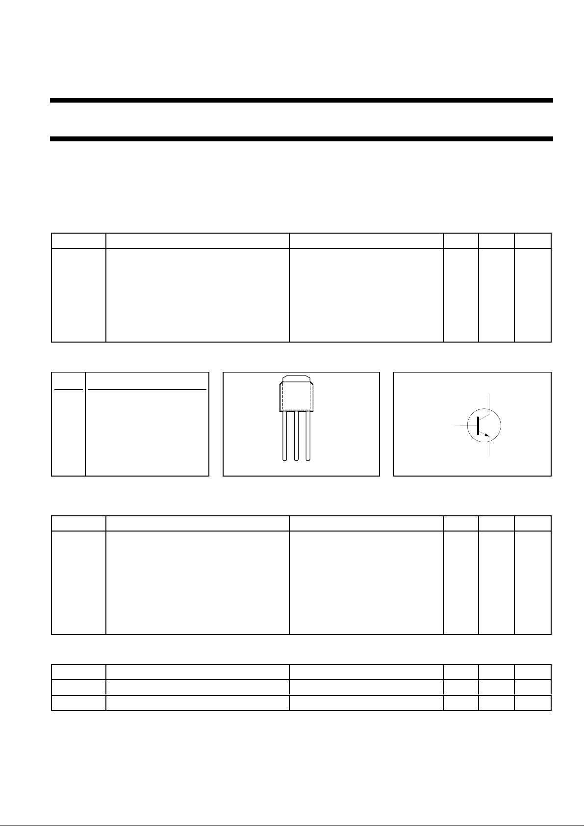
PINNING - SOT533 PIN CONFIGURATION SYMBOL
Collector-emitter voltage peak value VBE = 0 V - 700 V
Collector-base voltage (open emitter) - 700 V
Collector-emitter voltage (open base) - 400 V
Collector current (DC) - 4 A
Collector current peak value - 8 A
Total power dissipation Tmb ≤ 25 ˚C - 50 W
Collector-emitter saturation voltage IC = 3.0 A;IB = 0.6 A 0.25 1.0 V
D.C. current gain IC = 3.0 A; VCE = 5 V 12.5 Fall time IC = 2.5 A; IB1= 0.4 A 46 60 ns
PIN DESCRIPTION
c
1 base
2 collector
b
3 emitter
1
tab collector
LIMITING VALUES
Limiting values in accordance with the Absolute Maximum Rating System (IEC 134)
SYMBOL PARAMETER CONDITIONS MIN. MAX. UNIT
V
V
V
I
C
I
CM
I
B
I
BM
P
T
T
CESM
CEO
CBO
tot
stg
j
Collector to emitter voltage VBE = 0 V - 700 V
Collector to emitter voltage (open base) - 400 V
Collector to base voltage (open emitter) - 700 V
Collector current (DC) - 4 A
Collector current peak value - 8 A
Base current (DC) - 2 A
Base current peak value - 4 A
Total power dissipation Tmb ≤ 25 ˚C - 50 W
Storage temperature -65 150 ˚C
Junction temperature - 150 ˚C
THERMAL RESISTANCES
Top view
23
MBK915
e
SYMBOL PARAMETER CONDITIONS TYP. MAX. UNIT
R
R
th j-mb
th j-a
Junction to mounting base - 2.5 K/W
Junction to ambient in free air 70 - K/W
October 1999 1 Rev 1.100

Philips Semiconductors Product specification
Silicon Diffused Power Transistor BUJ103AU
STATIC CHARACTERISTICS
Tmb = 25 ˚C unless otherwise specified
SYMBOL PARAMETER CONDITIONS MIN. TYP. MAX. UNIT
I
CES,ICBO
I
CES
I
CEO
I
EBO
V
CEOsust
V
CEsat
V
BEsat
h
FE
h
FE
h
FEsat
Collector cut-off current
Collector cut-off current
Emitter cut-off current VEB = 7 V; IC = 0 A - - 0.1 mA
Collector-emitter sustaining voltage IB = 0 A; IC = 10 mA; 400 - - V
Collector-emitter saturation voltage IC = 3.0 A; IB = 0.6 A - 0.25 1.0 V
Base-emitter saturation voltage IC = 3.0 A; IB = 0.6 A - 0.97 1.5 V
DC current gain IC = 1 mA; VCE = 5 V 10 17 32
DYNAMIC CHARACTERISTICS
Tmb = 25 ˚C unless otherwise specified
SYMBOL PARAMETER CONDITIONS TYP. MAX. UNIT
Switching times (resistive load) I
t
on
t
s
t
f
t
s
t
f
t
s
t
f
Turn-on time 0.48 0.6 µs
Turn-off storage time 2.7 3.3 µs
Turn-off fall time 0.27 0.35 µs
Switching times (inductive load) I
Turn-off storage time 1.2 1.4 µs
Turn-off fall time 46 60 ns
Switching times (inductive load) I
Turn-off storage time 1.34 1.8 µs
Turn-off fall time 98 200 ns
1
1
VBE = 0 V; VCE = V
VBE = 0 V; VCE = V
Tj = 125 ˚C
V
CEO
= V
(400V) - - 0.1 mA
CEOMmax
CESMmax
; - - 0.5 mA
CESMmax
- - 0.1 mA
L = 25 mH
IC = 500mA; VCE = 5 V 13 22 32
IC = 2.0 A; VCE = 5 V 11 16 22
IC = 3.0 A; VCE = 5 V - 12.5 -
= 2.5 A; I
Con
RL = 75 ohms; V
= 2.5 A; I
Con
-VBB = 5 V
= 2.5 A; I
Con
-VBB = 5 V; Tj = 100 ˚C
= -I
Bon
Bon
Bon
= 0.5 A;
Boff
= 4V;
BB2
= 0.5 A; LB = 1 µH;
= 0.5 A; LB = 1 µH;
1 Measured with half sine-wave voltage (curve tracer).
October 1999 2 Rev 1.100
Philips Semiconductors Product specification
Silicon Diffused Power Transistor BUJ103AU
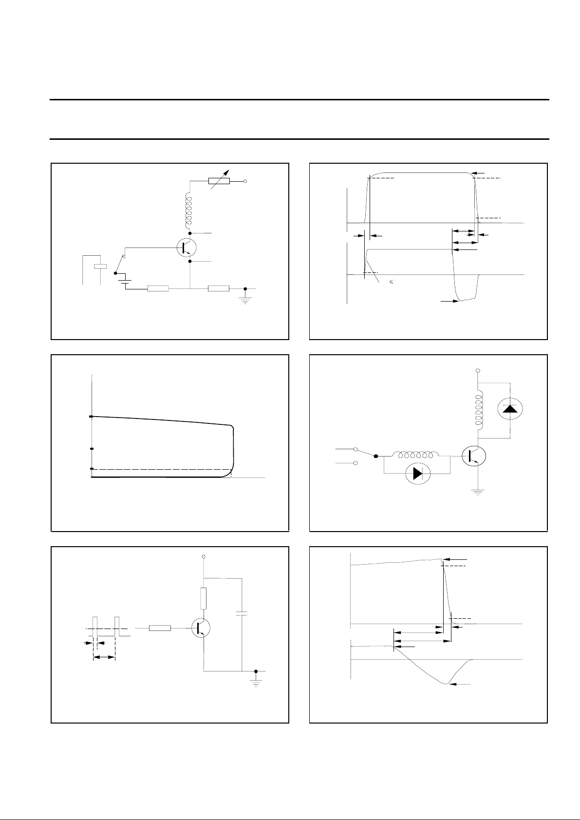
30-60 Hz
6V
Fig.1. Test circuit for V
IC / mA
250
100
10
0
Fig.2. Oscilloscope display for V
300R
VCE / V
100-200R
Horizontal
Oscilloscope
Vertical
1R
.
CEOsust
min
VCEOsust
CEOsust
+ 50v
.
LC
ts
toff
ICon
tf
IBon
VCC
Fig.
IC
IB
4.
Switching times waveforms with resistive load.
IBon
-VBB
Fig.
90 %
ton
10 %
tr
30ns
-IBoff
LB
5.
Test circuit inductive load.
VCC = 300 V; -VBE = 5 V, LC = 200 uH; LB = 1 uH
90 %
10 %
T.U.T.
tf
ICon
90 %
10 %
t
t
-IBoff
Fig
VIM
0
tp
T
.3.
Test circuit resistive load. VIM = -6 to +8 V
R
B
VCC
R
L
T.U.T.
IC
ts
toff
IB
Fig.
6.
Switching times waveforms with inductive load.
IBon
VCC = 250 V; tp = 20 µs; δ = tp / T = 0.01.
RB and RL calculated from I
Con
and I
requirements.
Bon
October 1999 3 Rev 1.100
 Loading...