

Philips BUJ100AT Datasheet
Philips Semiconductors Product specification
Silicon Diffused Power Transistor BUJ100AT
GENERAL DESCRIPTION
High-voltage, high-speed planar-passivated npn power switching transistor in the SOT223 envelope intended for
use in compact fluorescent lamps, low power electronic lighting ballasts and similar high frequency converters and
inverters.
QUICK REFERENCE DATA
SYMBOL PARAMETER CONDITIONS TYP. MAX. UNIT
V
CESM
V
CBO
V
CEO
I
C
I
CM
P
tot
V
CEsat
h
FE
t
fi
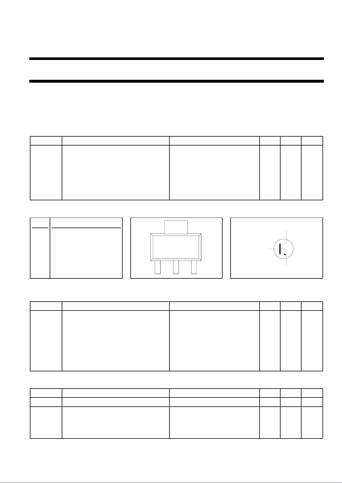
PINNING - SOT223 PIN CONFIGURATION SYMBOL
Collector-emitter voltage peak value VBE = 0 V - 700 V
Collector-Base voltage (open emitter) - 700 V
Collector-emitter voltage (open base) - 400 V
Collector current (DC) - 1.0 A
Collector current peak value - 2.0 A
Total power dissipation Tsp ≤ 25 ˚C - 6 W
Collector-emitter saturation voltage IC = 0.75 A;IB = 150 mA 0.23 1.0 V
IC = 0.75 A;VCE = 5 V 14 20
Fall time (Inductive) IC = 1.0 A,I
=200 mA 50 70 ns
BON
PIN DESCRIPTION
4
c
1 base
2 collector
b
3 emitter
4 collector (tab)
1
LIMITING VALUES
Limiting values in accordance with the Absolute Maximum Rating System (IEC 134)
SYMBOL PARAMETER CONDITIONS MIN. MAX. UNIT
V
V
V
I
C
I
CM
I
B
I
BM
P
T
T
CESM
CEO
CBO
tot
stg
j
Collector to emitter voltage VBE = 0 V - 700 V
Collector to emitter voltage (open base) - 400 V
Collector to base voltage (open emitter) - 700 V
Collector current (DC) - 1.0 A
Collector current peak value - 2.0 A
Base current (DC) - 0.5 A
Base current peak value - 1.0 A
Total power dissipation Tsp ≤ 25 ˚C - 6 W
Storage temperature -65 150 ˚C
Junction temperature - 150 ˚C
THERMAL RESISTANCES
23
e
SYMBOL PARAMETER CONDITIONS TYP. MAX. UNIT
R
R
th j-sp
th j-a
Junction to solder point - 20 K/W
Junction to ambient pcb mounted pad areas as in Fig.
23)
pcb mounted, minimum footprint 70 - K/W
Mounted on 50x34x2mm
aluminium PCB 30 - K/W
September 1999 1 Rev 1.000

Philips Semiconductors Product specification
Silicon Diffused Power Transistor BUJ100AT
STATIC CHARACTERISTICS
Tsp = 25 ˚C unless otherwise specified
SYMBOL PARAMETER CONDITIONS MIN. TYP. MAX. UNIT
I
CES,ICBO
I
CES
I
CEO
I
EBO
V
CEOsust
V
CEsat
V
BEsat
Collector cut-off current
Collector cut-off current VCE = V
Emitter cut-off current VEB = 9 V; IC = 0 A - 0.02 100 µA
Collector-emitter sustaining voltage IB = 0 A; IC = 10 mA; 400 - - V
Collector-emitter saturation voltage IC = 0.75 A; IB = 0.15mA - 0.23 1.0 V
Base-emitter saturation voltage IC = 0.75 A; IB = 0.15mA - 0.95 1.3 V
1
VBE = 0 V; VCE = V
VBE = 0 V; VCE = V
Tj = 125 ˚C
(400V) - - 100 µA
CESMmax
CESMmax
; - 15 500 µA
CESMmax
- 2.5 100 µA
L = 25 mH
h
FE
h
FE
h
FE
DC current gain IC = 10mA; VCE = 5 V 11 20 27
IC = 100mA; VCE = 5 V 12.5 21 31
IC = 0.75A; VCE = 5 V 9 14 20
DYNAMIC CHARACTERISTICS
Tsp = 25 ˚C unless otherwise specified
SYMBOL PARAMETER CONDITIONS TYP. MAX. UNIT
Switching times (resistive load) I
t
on
t
s
t
f
Turn-on time 0.65 0.88 µs
Turn-off storage time 0.88 1.2 µs
Turn-off fall time 250 338 ns
Switching times (inductive load) I
t
s
t
f
Turn-off storage time 0.51 0.7 µs
Turn-off fall time 50 70 ns
Switching times (inductive load) I
t
s
t
f
Turn-off storage time - 1.4 µs
Turn-off fall time - 130 ns
= 1.0 A; I
Con
RL = 75 ohms; V
= 1.0 A; I
Con
-VBB = 5 V
= 1.0 A; I
Con
= -I
Bon
Boff
= 4 V;
BB2
= 200mA; LB = 1 µH;
Bon
= 200mA; LB = 1 µH;
Bon
-VBB = 5 V; Tj = 100 ˚C
= 200mA;
1 Measured with half sine-wave voltage (curve tracer).
September 1999 2 Rev 1.000
Philips Semiconductors Product specification
Silicon Diffused Power Transistor BUJ100AT
30-60 Hz
IC / mA
250
100
6V
300R
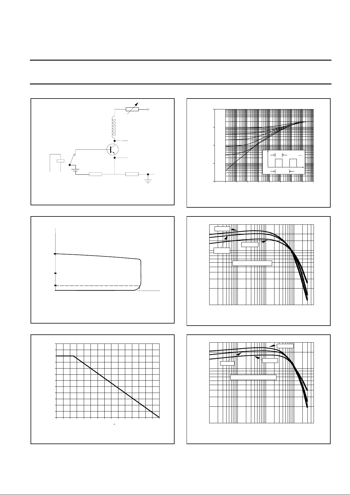
Fig.1. Test circuit for V
100-200R
Horizontal
Oscilloscope
Vertical
1R
.
CEOsust
+ 50v
!
Zth / (K/W)
100
10
0.5
0.2
0.1
1
0.05
0.02
t
p
P
D
0.1
0.01
D=0
1u 100u 10m 1 100
10u 1m 100m 10
T
t / s
Fig.4. Transient thermal impedance.
Zth
HFE
30
125 C
20
15
10
25 C
5
= f(t); parameter D = tp/T
j-lead
-40 C
VCE = 1V
D =
t
p
T
t
10
0
VCE / V
VCEOsust
Fig.2. Oscilloscope display for V
PD%
120
110
100
90
80
70
60
50
40
30
20
10
0
0 20 40 60 80 100 120 140
Normalised Power Derating
Tmb / C
Fig.3. Normalised power dissipation.
PD% = 100⋅PD/PD
= f (Tmb)
25˚C
min
CEOsust
1
.
0.001 0.01 0.1 1 2 3 5
IC/A
Fig.5. Typical DC current gain. hFE = f(IC)
parameter V
HFE
30
10
25 C
VCE = 5V
1
0.001 0.01 0.1 1 2 3 5
CE
125 C
-40 C
IC/A
Fig.6. Typical DC current gain. hFE = f(IC)
parameter V
CE
September 1999 3 Rev 1.000
 Loading...