

Philips BU506DF Datasheet

DISCRETE SEMICONDUCTORS
DATA SH EET
BU506F; BU506DF
Silicon diffused power transistors
Product specification
Supersedes data of February 1996
File under Discrete Semiconductors, SC06
1997 Aug 14
Philips Semiconductors Product specification
Silicon diffused power transistors BU506F; BU506DF
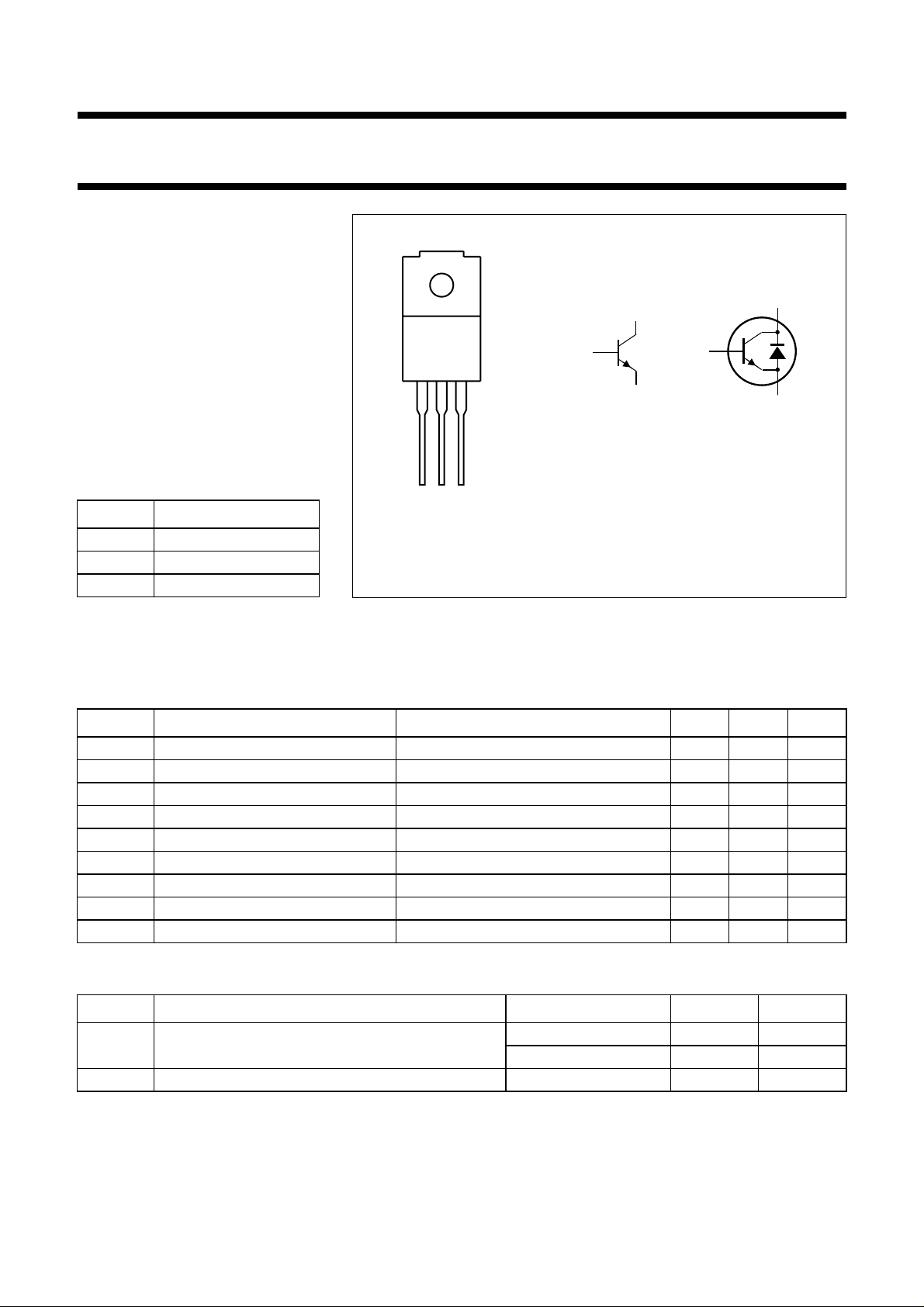
DESCRIPTION
High-voltage, high-speed switching
NPN power transistor in a SOT186
package. The BU506DF has an
integrated efficiency diode.
2
2
APPLICATIONS
1
1
• Horizontal deflection circuits of
colour television receivers
MBB008
3
MBB077
3
• Line-operated switch-mode
applications.
a. BU506F. b. BU506DF.
PINNING
(1)
PIN
DESCRIPTION
123
Front view
MBC668
1 base
2 collector
Fig.1 Simplified outline (SOT186) and symbols.
3 emitter
Note
1. All pins electrically isolated from mounting base.
QUICK REFERENCE DATA
SYMBOL PARAMETER CONDITIONS TYP. MAX. UNIT
V
CESM
V
CEO
V
CEsat
V
F
I
Csat
I
C
I
CM
P
tot
t
f
collector-emitter peak voltage VBE=0 − 1500 V
collector-emitter voltage open base − 700 V
collector-emitter saturation voltage IC= 3 A; IB= 1.33 A; see Figs 7 and 8 − 1V
diode forward voltage (BU506DF) IF= 3 A 1.5 2.2 V
collector saturation current − 3A
collector current (DC) see Figs 2 and 3 − 5A
collector current (peak value) see Figs2and3 − 8A
total power dissipation Th≤ 25 °C; see Fig.4 − 20 W
fall time inductive load; see Fig.11 0.7 −µs
THERMAL CHARACTERISTICS
SYMBOL PARAMETER CONDITIONS VALUE UNIT
R
th j-h
thermal resistance from junction to external heatsink note 1 6.35 K/W
note 2 3.85 K/W
R
th j-a
thermal resistance from junction to ambient 55 K/W
Notes
1. Mounted without heatsink compound and 30 ±5 N force on centre of package.
2. Mounted with heatsink compound and 30 ±5 N force on centre of package.
1997 Aug 14 1

Philips Semiconductors Product specification
Silicon diffused power transistors BU506F; BU506DF
LIMITING VALUES
In accordance with the Absolute Maximum Rating System (IEC 134).
SYMBOL PARAMETER CONDITIONS MIN. MAX. UNIT
V
CESM
V
CEO
I
Csat
I
C
I
CM
I
B
I
BM
P
tot
T
stg
T
j
collector-emitter peak voltage VBE=0 − 1500 V
collector-emitter voltage open base − 700 V
collector saturation current VCE=5V − 3A
collector current (DC) see Figs 2 and 3 − 5A
collector current (peak value) see Figs 2 and 3 − 8A
base current (DC) − 3A
base current (peak value) − 5A
total power dissipation Th≤ 25 °C; see Fig.4 − 20 W
storage temperature −65 +150 °C
junction temperature − 150 °C
ISOLATION CHARACTERISTICS
SYMBOL PARAMETER TYP. MAX. UNIT
V
C
isolM
isol
isolation voltage from all terminals to external heatsink (peak value) − 1500 V
isolation capacitance from collector to external heatsink 12 − pF
CHARACTERISTICS
T
=25°C unless otherwise specified.
j
SYMBOL PARAMETER CONDITIONS MIN. TYP. MAX. UNIT
V
CEOsust
V
CEsat
V
BEsat
V
F
I
CES
collector-emitter sustaining
voltage
collector-emitter saturation
voltage
IC= 100 mA; IB= 0; L = 25 mH;
see Figs 5 and 6
IC= 3 A; IB= 1.33 A;
see Figs 7 and 8
700 −−V
−−1V
base-emitter saturation voltage IC= 3 A; IB= 1.33 A; see Fig.9 −−1.3 V
diode forward voltage (BU506DF) IF=3A − 1.5 2.2 V
collector-emitter cut-off current VCE=V
V
CE=VCESmax
; VBE=0 −−0.5 mA
CESmax
; VBE=0;
−−1mA
Tj= 125 °C
I
EBO
h
FE
emitter-base cut-off current VEB=6V; IC=0 −−10 mA
DC current gain VCE=5V; IC= 3 A; see Fig.10 2.25 −−
V
=5V; IC= 100 mA;
CE
61330
see Fig.10
Switching times in horizontal deflection circuit (see Fig.11)
t
s
t
f
storage time I
fall time I
=3A;LB=12µH;
Csat
I
= 1 A; dIB/dt = −0.33 A/µs
B(end)
=3A;LB=12µH;
Csat
I
= 1 A; dIB/dt = −0.33 A/µs
B(end)
1997 Aug 14 2
− 6.5 −µs
− 0.7 −µs
Philips Semiconductors Product specification
Silicon diffused power transistors BU506F; BU506DF
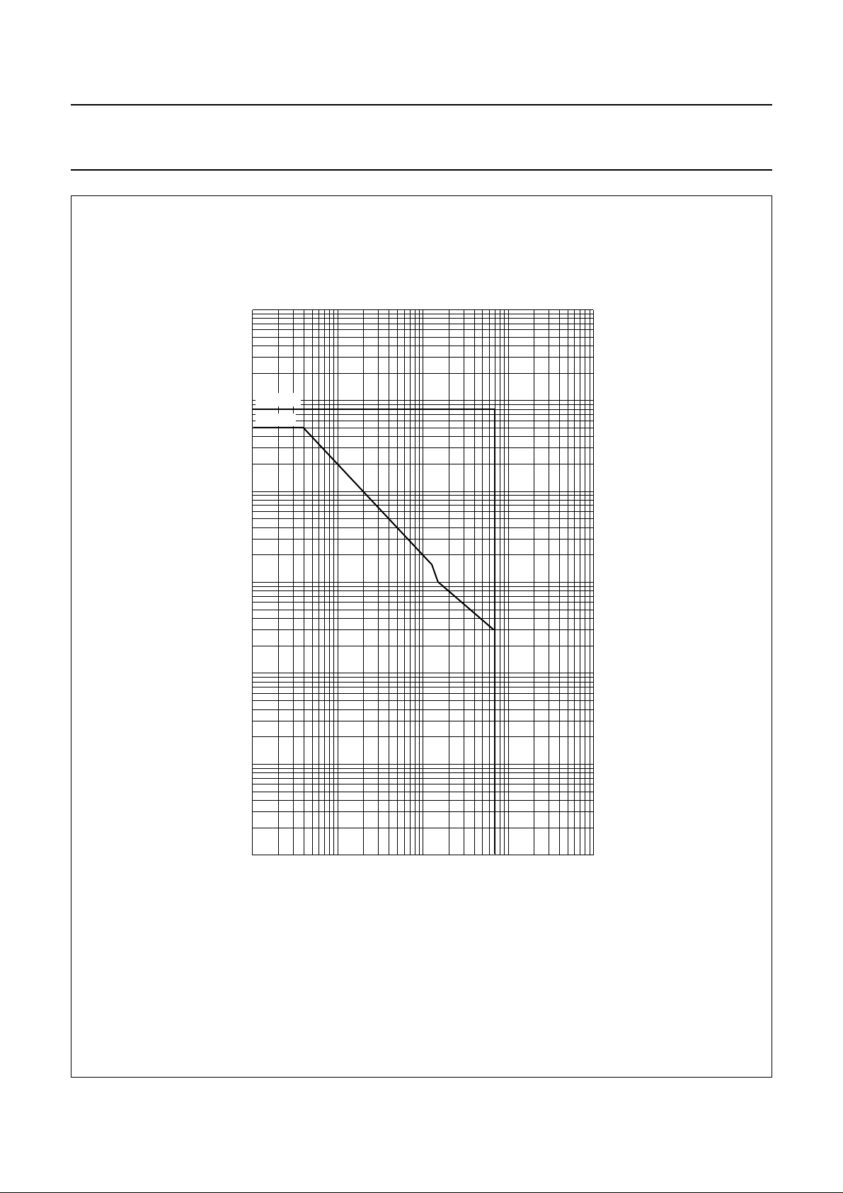
handbook, full pagewidth
10
10
(A)
2
10
I
C
I
10
CM max
I
C max
II
1
−1
−2
I
MGB933
−3
10
−4
10
110
Mounted without heatsink compound and 30±5 N force on centre of package.
Tmb=25°C.
I -Region of permissible DC operation.
II -Permissible extension for repetitive pulse operation.
10
Fig.2 Forward bias SOAR (no heatsink compound).
1997 Aug 14 3
2
3
10
VCE (V)
4
10
 Loading...