

Philips BU4530AW Datasheet
Philips Semiconductors Object specification
Silicon Diffused Power Transistor BU4530AW
GENERAL DESCRIPTION
Enhanced performance, new generation, high-voltage, high-speed switching npn transistor in a plastic envelope
intended for use in horizontal deflection circuits of colour television receivers and p.c monitors. Features exceptional
tolerance to base drive and collector current load variations resulting in a very low worst case dissipation.
QUICK REFERENCE DATA
SYMBOL PARAMETER CONDITIONS TYP. MAX. UNIT
V
CESM
V
CEO
I
C
I
CM
P
tot
V
CEsat
I
Csat
t
f
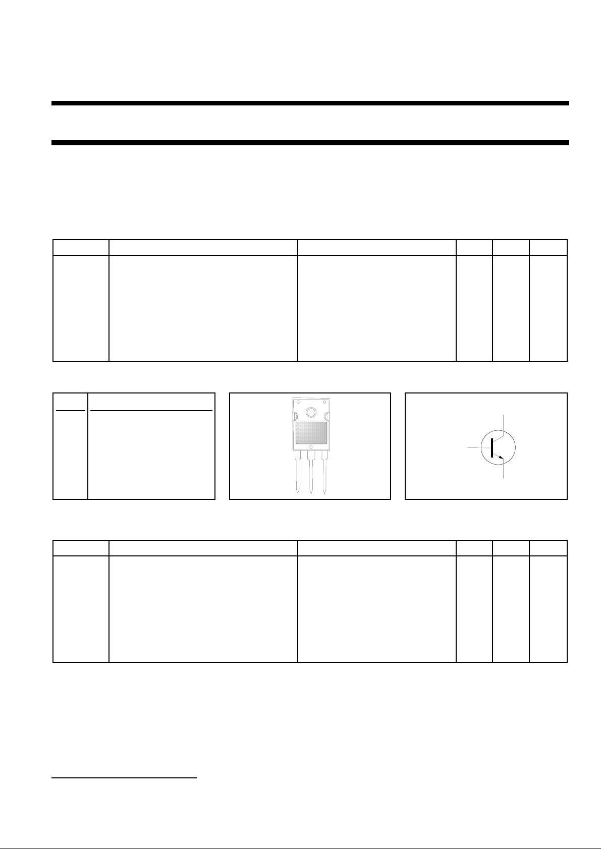
PINNING - SOT429 PIN CONFIGURATION SYMBOL
Collector-emitter voltage peak value VBE = 0 - 1500 V
Collector-emitter voltage (open base) - 800 V
Collector current (DC) - 16 A
Collector current peak value - 40 A
Total power dissipation Tmb ≤ 25 ˚C - 125 W
Collector-emitter saturation voltage IC = 10.0 A; IB = 2.5 A - 3.0 V
Collector saturation current f = 32 kHz 10 - A
f = 90 kHz 8 - A
Fall time I
= 10.0 A; f = 32 kHz t.b.f t.b.f µs
Csat
I
= 8 A; f = 90 kHz t.b.f t.b.f µs
Csat
PIN DESCRIPTION
c
1 base
2 collector
b
3 emitter
tab collector
LIMITING VALUES
Limiting values in accordance with the Absolute Maximum Rating System (IEC 134)
SYMBOL PARAMETER CONDITIONS MIN. MAX. UNIT
V
V
I
C
I
CM
I
B
I
BM
-I
P
T
T
CESM
CEO
BM
tot
stg
j
Collector-emitter voltage peak value VBE = 0 V - 1500 V
Collector-emitter voltage (open base) - 800 V
Collector current (DC) - 16 A
Collector current peak value - 40 A
Base current (DC) - 10 A
Base current peak value - 15 A
Reverse base current peak value
1
Total power dissipation Tmb ≤ 25 ˚C - 125 W
Storage temperature -55 150 ˚C
Junction temperature - 150 ˚C
2
1
3
e
-10A
1 Turn-off current.
January 1998 1 Rev 1.000

Philips Semiconductors Object specification
Silicon Diffused Power Transistor BU4530AW
THERMAL RESISTANCES
SYMBOL PARAMETER CONDITIONS TYP. MAX. UNIT
R
th j-mb
R
th j-a
STATIC CHARACTERISTICS
Tmb = 25 ˚C unless otherwise specified
SYMBOL PARAMETER CONDITIONS MIN. TYP. MAX. UNIT
I
CES
I
CES
I
EBO
BV
EBO
V
CEsat
V
BEsat
h
FE
h
FE
Junction to mounting base - - 1.0 K/W
Junction to ambient in free air 45 - K/W
Collector cut-off current
2
VBE = 0 V; VCE = V
VBE = 0 V; VCE = V
Tj = 125 ˚C
CESMmax
; - - 2.0 mA
CESMmax
- - 1.0 mA
Emitter cut-off current VEB = 7.5 V; IC = 0 A - - 1.0 mA
Base-emitter breakdown voltage IB = 1 mA 7.5 14 - V
Collector-emitter saturation voltage IC = 10.0 A; IB = 2.5 A - - 3.0 V
Base-emitter saturation voltage IC = 10.0 A; IB = 2.5 A t.b.f - 1.0 V
DC current gain IC = 1 A; VCE = 5 V - t.b.f -
IC = 10 A; VCE = 5 V 4.2 5.35 6.5
DYNAMIC CHARACTERISTICS
Tmb = 25 ˚C unless otherwise specified
SYMBOL PARAMETER CONDITIONS TYP. MAX. UNIT
Switching times (32 kHz line I
deflection dynamic test circuit).
t
s
t
f
Turn-off storage time t.b.f t.b.f µs
Turn-off fall time t.b.f t.b.f µs
Switching times (90 kHz line I
deflection dynamic test circuit).
t
s
t
f
Turn-off storage time t.b.f t.b.f µs
Turn-off fall time t.b.f t.b.f µs
= 10.0 A;IB1 = 2A;(IB2 = -5A)
Csat
= 8 A;IB1 = 1.6A;(IB2 = -4.8A)
Csat
2 Measured with half sine-wave voltage (curve tracer).
January 1998 2 Rev 1.000
 Loading...