

Philips BU4525DL Datasheet
Philips Semiconductors Product specification
Silicon Diffused Power Transistor BU4525DL
GENERAL DESCRIPTION
Enhanced performance, new generation, high-voltage, high-speed switching npn transistor in a plastic envelope
with integrated damper diode intended intended for use in horizontal deflection circuits of colour television receivers
and p.c monitors. Features exceptional tolerance to base drive and collector current load variations resulting in a
very low worst case dissipation.
QUICK REFERENCE DATA
SYMBOL PARAMETER CONDITIONS TYP. MAX. UNIT
V
V
I
I
P
V
V
I
t
C
CM
Csat
f
CESM
CEO
tot
CEsat
F
Collector-emitter voltage peak value VBE = 0 V - 1500 V
Collector-emitter voltage (open base) - 800 V
Collector current (DC) - 14 A
Collector current peak value - 30 A
Total power dissipation Ths ≤ 25 ˚C - 125 W
Collector-emitter saturation voltage IC = 9.0 A; IB = 2.25 A - 3.0 V
Diode forward voltage IF = 9.0 A - 2.2 V
Collector saturation current f = 16 kHz 9.0 - A
f = 70 kHz t.b.f - A
Fall time I
= 9.0 A;f = 16 kHz 0.4 0.55 µs
Csat
f = 70 kHz t.b.f t.b.f µs
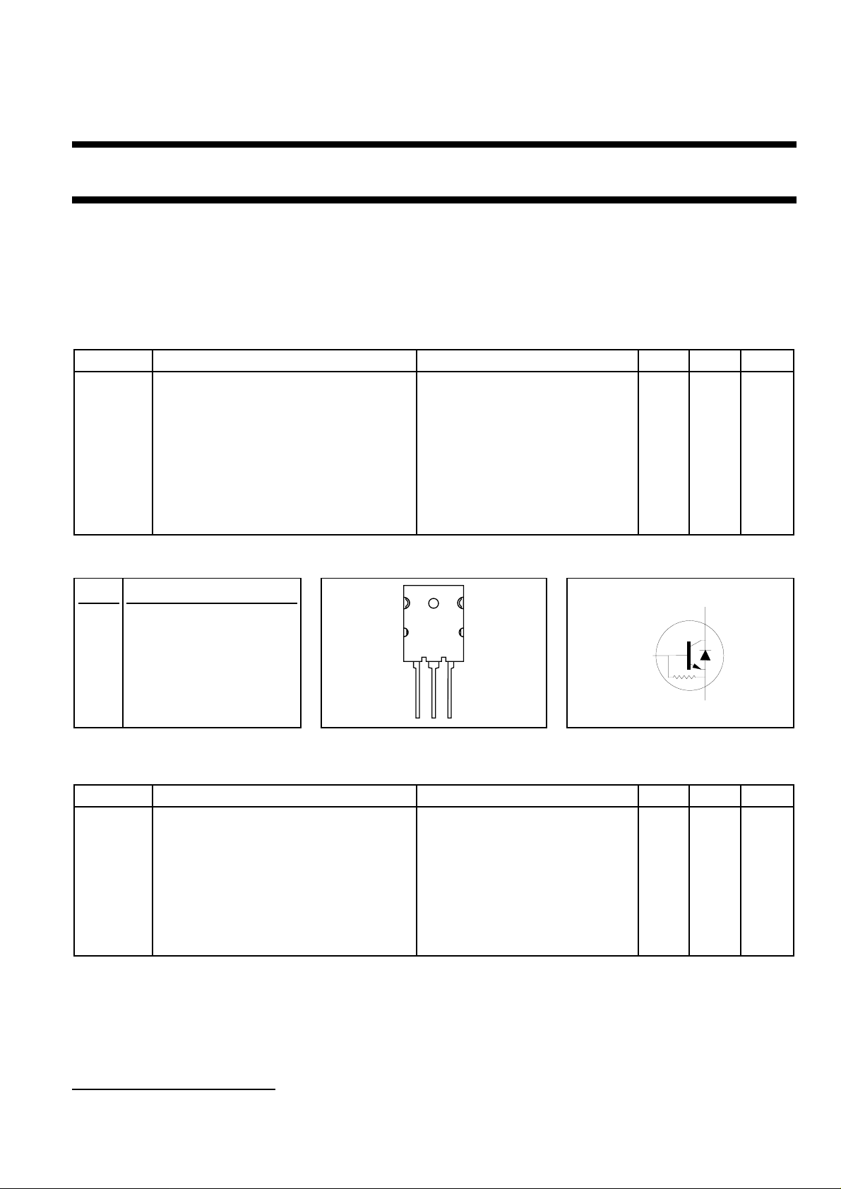
PINNING - SOT430 PIN CONFIGURATION SYMBOL
PIN DESCRIPTION
1 base
2 collector
c
b
3 emitter
heat collector
sink
123
LIMITING VALUES
Limiting values in accordance with the Absolute Maximum Rating System (IEC 134)
SYMBOL PARAMETER CONDITIONS MIN. MAX. UNIT
V
V
I
C
I
CM
I
B
I
BM
-I
P
T
T
CESM
CEO
BM
tot
stg
j
Collector-emitter voltage peak value VBE = 0 V - 1500 V
Collector-emitter voltage (open base) - 800 V
Collector current (DC) - 14 A
Collector current peak value - 30 A
Base current (DC) - 8 A
Base current peak value - 12 A
Reverse base current peak value
1
Total power dissipation Ths ≤ 25 ˚C - 125 W
Storage temperature -55 150 ˚C
Junction temperature - 150 ˚C
Rbe
e
-7A
1 Turn-off current.
July 1998 1 Rev 1.000
Philips Semiconductors Objective specification
Silicon Diffused Power Transistor BU4525DL
THERMAL RESISTANCES
SYMBOL PARAMETER CONDITIONS TYP. MAX. UNIT
R
th j-hs
R
th j-a
STATIC CHARACTERISTICS
Ths = 25 ˚C unless otherwise specified
SYMBOL PARAMETER CONDITIONS MIN. TYP. MAX. UNIT
I
CES
I
CES
BV
EBO
R
be
V
CEOsust
V
CEsat
V
BEsat
h
FE
h
FE
V
F
Junction to heatsink with heatsink compound - 1 K/W
Junction to ambient in free air 45 - K/W
Collector cut-off current
2
VBE = 0 V; VCE = V
VBE = 0 V; VCE = V
Tj = 125 ˚C
CESMmax
; - - 2.0 mA
CESMmax
- - 1.0 mA
Emitter-base breakdown voltage IB = 600 mA 7.5 13.5 - V
Base-emitter resistance VEB = 7.5 V - 50 - Ω
Collector-emitter sustaining voltage IB = 0 A; IC = 100 mA; 800 - - V
L = 25 mH
Collector-emitter saturation voltage IC = 9.0 A;IB = 2.25A - - 3.0 V
Base-emitter saturation voltage IC = 9.0 A;IB = 2.25A 0.96 1.01 1.06 V
DC current gain IC = 1.0 A; VCE = 5 V - 12 -
IC = 9.0 A; VCE = 5 V 4.2 5.8 7.6
Diode forward voltage IF = 9 A - - 2.2 V
DYNAMIC CHARACTERISTICS
Ths = 25 ˚C unless otherwise specified
SYMBOL PARAMETER CONDITIONS TYP. MAX. UNIT
C
c
t
s
t
f
t
s
t
f
Collector capacitance IE = 0 A; VCB = 10 V; f = 1 MHz 145 - pF
Switching times (16 kHz line I
deflection circuit) (IB2 = -4.5 A)
= 9.0 A;IB1 = 1.8 A
Csat
Turn-off storage time 3.7 4.5 µs
Turn-off fall time 0.4 0.55 µs
Switching times (70 kHz line I
deflection circuit)
Csat
= t.b.f
Turn-off storage time t.b.f t.b.f µs
Turn-off fall time t.b.f t.b.f µs
2 Measured with half sine-wave voltage (curve tracer).
July 1998 2 Rev 1.000
 Loading...