

Philips bu4508af DATASHEETS

DISCRETE SEMICONDUCTORS
DATA SH EET
BU4508AF
Silicon Diffused Power Transistor
Product specification
Supersedes data of January 1998
File under Discrete Semiconductors, SC06
June 1998
Philips Semiconductors Product specification
Silicon Diffused Power Transistor BU4508AF
GENERAL DESCRIPTION
Enhanced performance, new generation, high-voltage, high-speed switching npn transistor in a plastic full-pack
envelope intended for use in horizontal deflection circuits of colour television receivers an p.c monitors. Features
exceptional tolerance to base drive and collector current load variations resulting in a very low worst case
dissipation.
QUICK REFERENCE DATA
SYMBOL PARAMETER CONDITIONS TYP. MAX. UNIT
V
V
I
I
P
V
I
t
C
CM
Csat
f
CESM
CEO
tot
CEsat
Collector-emitter voltage peak value VBE = 0 V - 1500 V
Collector-emitter voltage (open base) - 800 V
Collector current (DC) - 8 A
Collector current peak value - 15 A
Total power dissipation Ths ≤ 25 ˚C - 45 W
Collector-emitter saturation voltage IC = 5.0 A; IB = 1.25 A - 3.0 V
Collector saturation current f = 16kHz 5.0 - A
f = 64kHz 4.0 - A
Fall time I
= 5A; f = 16kHz 0.35 0.48 µs
Csat
= 4A; f = 64kHz 0.17 - µs
I
Csat
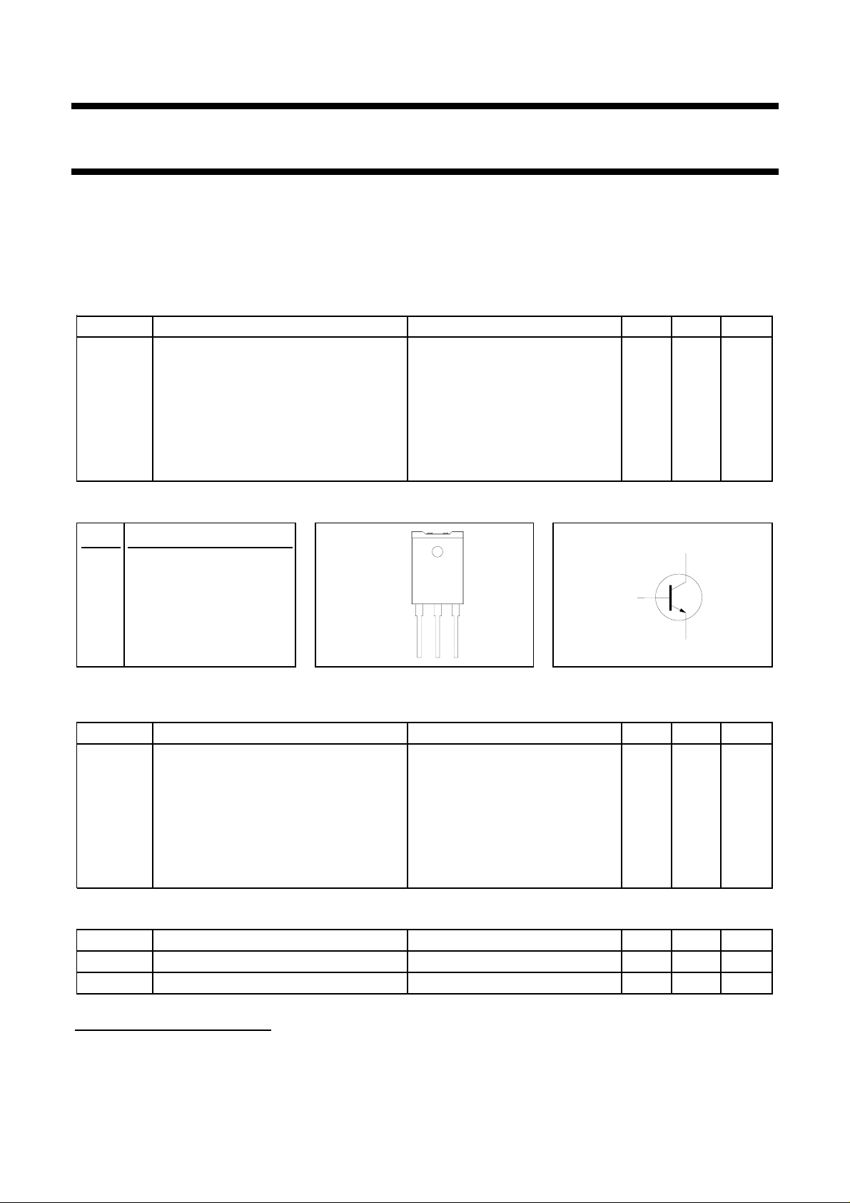
PINNING - SOT199 PIN CONFIGURATION SYMBOL
PIN DESCRIPTION
1 base
2 collector
3 emitter
case isolated
case
12
b
3
c
e
LIMITING VALUES
Limiting values in accordance with the Absolute Maximum Rating System (IEC 134)
SYMBOL PARAMETER CONDITIONS MIN. MAX. UNIT
V
CESM
V
CEO
I
C
I
CM
I
B
I
BM
-I
BM
P
tot
T
stg
T
j
Collector-emitter voltage peak value VBE = 0 V - 1500 V
Collector-emitter voltage (open base) - 800 V
Collector current (DC) - 8 A
Collector current peak value - 15 A
Base current (DC) - 4 A
Base current peak value - 6 A
Reverse base current peak value
1
-5A
Total power dissipation Ths ≤ 25 ˚C - 45 W
Storage temperature -55 150 ˚C
Junction temperature - 150 ˚C
THERMAL RESISTANCES
SYMBOL PARAMETER CONDITIONS TYP. MAX. UNIT
R
th j-hs
R
th j-a
1 Turn-off current.
Junction to heatsink with heatsink compound - 2.8 K/W
Junction to ambient in free air 35 - K/W
June 1998 1 Rev 1.000

Philips Semiconductors Product specification
Silicon Diffused Power Transistor BU4508AF
ISOLATION LIMITING VALUE & CHARACTERISTIC
Ths = 25 ˚C unless otherwise specified
SYMBOL PARAMETER CONDITIONS MIN. TYP. MAX. UNIT
V
isol
C
isol
STATIC CHARACTERISTICS
Ths = 25 ˚C unless otherwise specified
SYMBOL PARAMETER CONDITIONS MIN. TYP. MAX. UNIT
I
CES
I
CES
I
EBO
BV
EBO
V
CEOsust
V
CEsat
V
BEsat
h
FE
h
FE
Repetitive peak voltage from all R.H. ≤ 65 % ; clean and dustfree - - 2500 V
three terminals to external
heatsink
Capacitance from T2 to external f = 1 MHz - 22 - pF
heatsink
Collector cut-off current
Emitter cut-off current VEB = 6.0 V; IC = 0 A - - 100 uA
2
VBE = 0 V; VCE = V
VBE = 0 V; VCE = V
T
= 125 ˚C
j
CESMmax
; - - 2.0 mA
CESMmax
- - 1.0 mA
Emitter-base breakdown voltage IB = 1 mA 7.5 13.5 - V
Collector-emitter sustaining voltage IB = 0 A; IC = 100 mA; 800 - - V
L = 25 mH
Collector-emitter saturation voltages IC = 5.0 A; IB = 1.25 A - - 3.0 V
Base-emitter saturation voltage IC = 5.0 A; IB = 1.25 A 0.85 0.94 1.03 V
DC current gain IC = 100 mA; VCE = 5 V - 12 -
IC = 5.0 A; VCE = 5 V 4.2 5.7 7.3
DYNAMIC CHARACTERISTICS
Ths = 25 ˚C unless otherwise specified
SYMBOL PARAMETER CONDITIONS TYP. MAX. UNIT
C
c
t
s
t
f
t
s
t
f
Collector capacitance IE = 0 A; VCB = 10 V; f = 1 MHz 80 - pF
Switching times (16 kHz line I
deflection circuit)
= 5.0 A; IB1 = 1.0 A;(IB2 = -2.5 A)
Csat
Turn-off storage time 3.2 4.3 µs
Turn-off fall time 0.35 0.48 µs
Switching times (64 kHz line I
deflection circuit)
= 4 A; IB1 = 0.8 A;(IB2 = -2.0 A)
Csat
Turn-off storage time 1.9 - µs
Turn-off fall time 0.17 - µs
2 Measured with half sine-wave voltage (curve tracer).
June 1998 2 Rev 1.000

Philips Semiconductors Product specification
Silicon Diffused Power Transistor BU4508AF
30-60 Hz
IC / mA
250
200
100
100R
6V
Fig.1. Test circuit for V
100-200R
Horizontal
Oscilloscope
Vertical
1R
.
CEOsust
+ 50v
IBend
ICsat
90 %
IC
10 %
IB
ts
IB1
tf
- IB2
Fig.4. Switching times definitions.
+ 150 v nominal
adjust for ICsat
Lc
LB
T.U.T.
Cfb
t
t
0
VCE / V
Fig.2. Oscilloscope display for V
TRANSISTOR
IC
IB
VCE
DIODE
26us20us
64us
min
VCEOsust
CEOsust
ICsat
IB1
IB2
.
t
t
t
Fig.3. Switching times waveforms (16 kHz).
-VBB
Fig.5. Switching times test circuit
hFE
100
VCE = 1V
10
1
0.001 0.01 0.1 1 10
Fig.6. High and low DC current gain.
Ths = 25 C
Ths = 85 C
.
IC / A
June 1998 3 Rev 1.000
 Loading...