

Philips BU2523DF Datasheet
Philips Semiconductors Product specification
Silicon Diffused Power Transistor BU2523DF
GENERAL DESCRIPTION
New generation, high-voltage, high-speed switching npn transistor with an integrated damper diode in a full plastic
envelope intended for use in horizontal deflection circuits of HDTV receivers and pc monitors.
QUICK REFERENCE DATA
SYMBOL PARAMETER CONDITIONS TYP. MAX. UNIT
V
CESM
V
CEO
I
C
I
CM
P
tot
V
CEsat
I
Csat
V
F
t
f
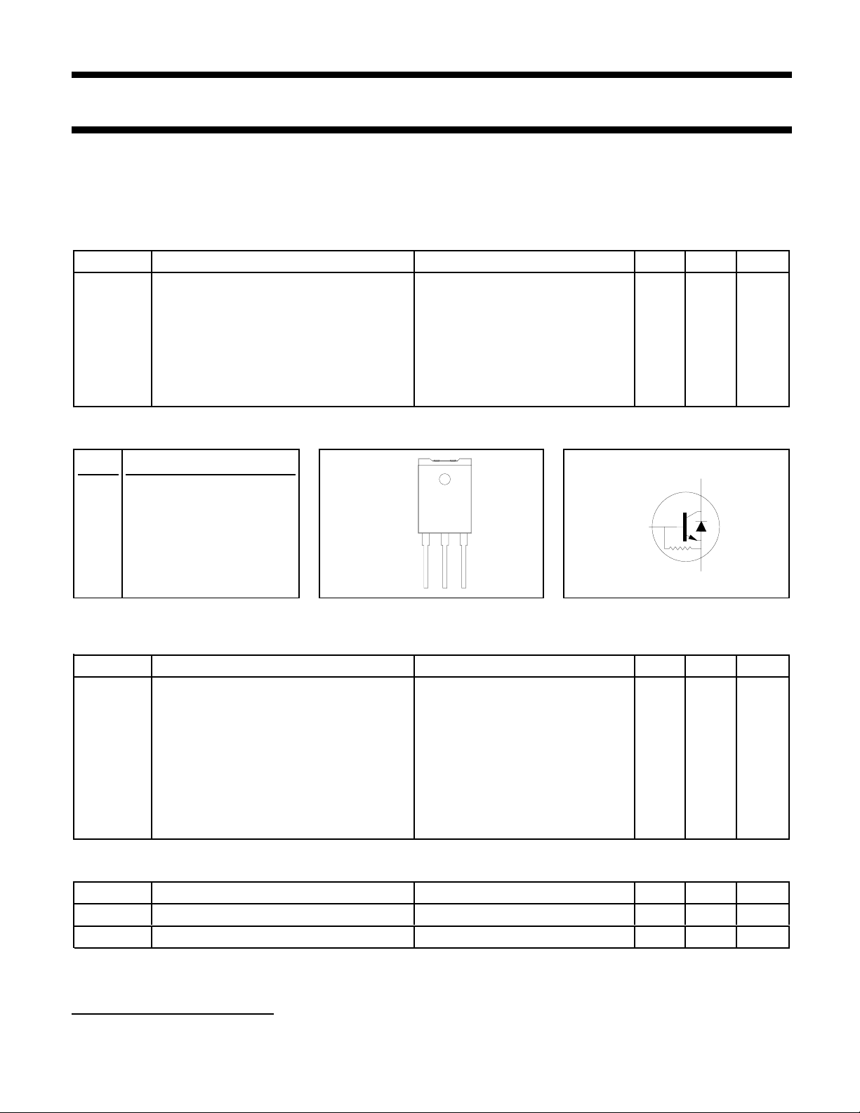
PINNING - SOT199 PIN CONFIGURATION SYMBOL
Collector-emitter voltage peak value VBE = 0 V - 1500 V
Collector-emitter voltage (open base) - 800 V
Collector current (DC) - 11 A
Collector current peak value - 29 A
Total power dissipation Ths ≤ 25 ˚C - 45 W
Collector-emitter saturation voltage IC = 5.5 A; IB = 1.1 A - 5.0 V
Collector saturation current f = 64 kHz 5.5 - A
Diode forward voltage IF = 5.5 A - 2.2 V
Fall time I
= 5.5 A; f = 64 kHz 0.15 0.3 µs
Csat
PIN DESCRIPTION
1 base
case
c
2 collector
b
3 emitter
case isolated
12
3
LIMITING VALUES
Limiting values in accordance with the Absolute Maximum Rating System (IEC 134)
SYMBOL PARAMETER CONDITIONS MIN. MAX. UNIT
V
CESM
V
CEO
I
C
I
CM
I
B
I
BM
-I
B(AV)
-I
BM
P
tot
T
stg
T
j
Collector-emitter voltage peak value VBE = 0 V - 1500 V
Collector-emitter voltage (open base) - 800 V
Collector current (DC) - 11 A
Collector current peak value - 29 A
Base current (DC) - 7 A
Base current peak value - 10 A
Reverse base current average over any 20 ms period - 175 mA
Reverse base current peak value
1
Total power dissipation Ths ≤ 25 ˚C - 45 W
Storage temperature -55 150 ˚C
Junction temperature - 150 ˚C
THERMAL RESISTANCES
Rbe
e
-7A
SYMBOL PARAMETER CONDITIONS TYP. MAX. UNIT
R
th j-hs
R
th j-a
1 Turn-off current.
Junction to heatsink with heatsink compound - 2.8 K/W
Junction to ambient in free air 35 - K/W
September 1997 1 Rev 1.200

Philips Semiconductors Product specification
Silicon Diffused Power Transistor BU2523DF
ISOLATION LIMITING VALUE & CHARACTERISTIC
Ths = 25 ˚C unless otherwise specified
SYMBOL PARAMETER CONDITIONS MIN. TYP. MAX. UNIT
V
isol
C
isol
STATIC CHARACTERISTICS
Ths = 25 ˚C unless otherwise specified
SYMBOL PARAMETER CONDITIONS MIN. TYP. MAX. UNIT
I
CES
I
CES
I
EBO
BV
EBO
V
CEOsust
R
be
V
CEsat
V
BEsat
h
FE
h
FE
V
F
Repetitive peak voltage from all R.H. ≤ 65 % ; clean and dustfree - 2500 V
three terminals to external
heatsink
Capacitance from T2 to external f = 1 MHz - 22 - pF
heatsink
Collector cut-off current
2
VBE = 0 V; VCE = V
VBE = 0 V; VCE = V
Tj = 125 ˚C
CESMmax
; - - 2.0 mA
CESMmax
- - 1.0 mA
Emitter cut-off current VEB = 6.0 V; IC = 0 A 80 130 170 mA
Emitter-base breakdown voltage IB = 600 mA 7.5 13.5 - V
Collector-emitter sustaining voltage IB = 0 A; IC = 100 mA; 800 - - V
L = 25 mH
Base-emitter resistance VEB = 7.5 V - 46 - Ω
Collector-emitter saturation voltage IC = 5.5 A; IB = 1.1 A - - 5.0 V
Base-emitter saturation voltage IC = 5.5 A; IB = 1.1 A - - 1.0 V
DC current gain IC = 1.0 A; VCE = 5 V - 12 -
IC = 5.5 A; VCE = 5 V 5 7.5 10.8
Diode forward voltage IF = 5.5 A - - 2.2 V
DYNAMIC CHARACTERISTICS
Ths = 25 ˚C unless otherwise specified
SYMBOL PARAMETER CONDITIONS TYP. MAX. UNIT
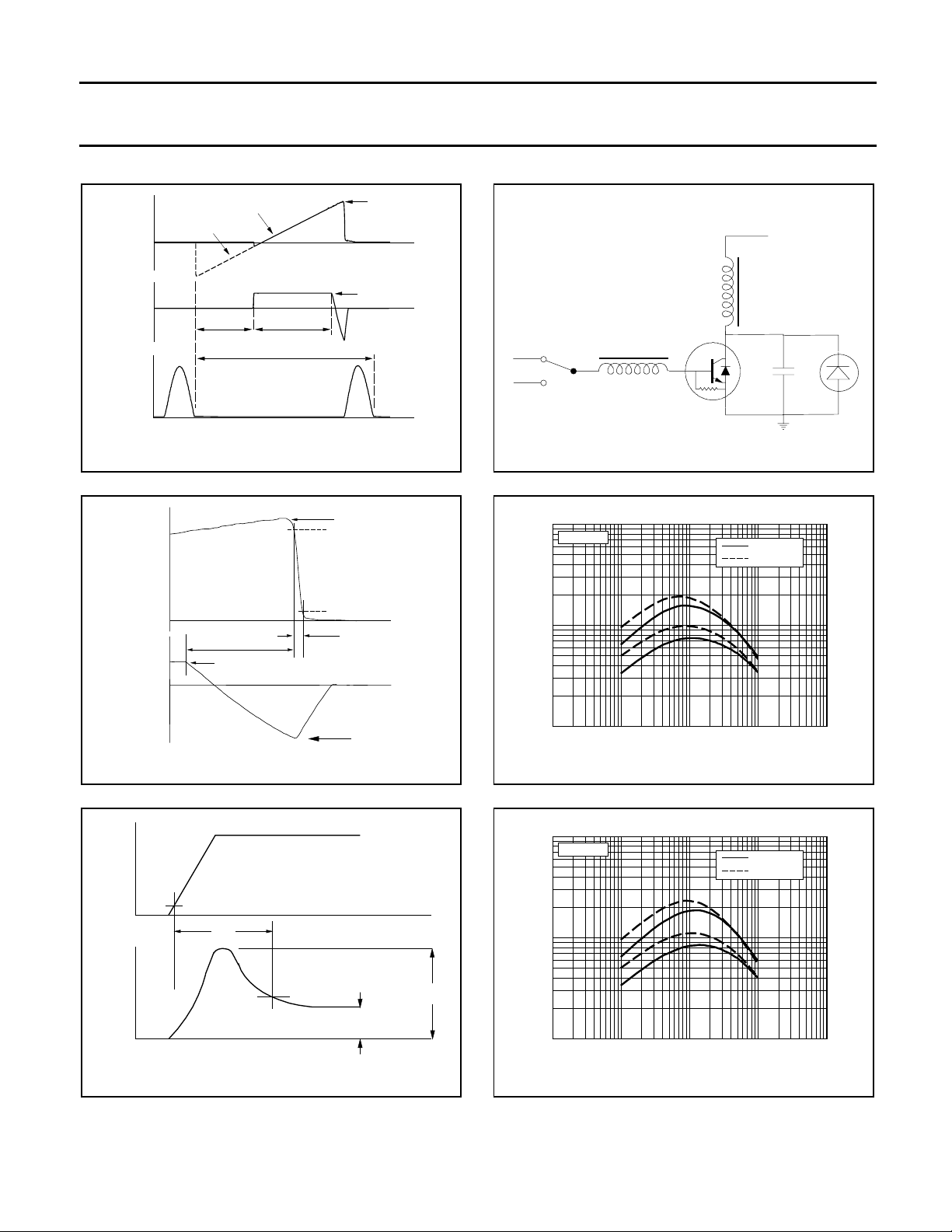
Switching times (64 kHz line I
deflection circuit) VCC = 145 V; I
t
s
t
f
V
fr
Turn-off storage time 1.5 2 µs
Turn-off fall time 0.15 0.3 µs
Anti-parallel diode forward recovery IF = 5.5 A; dIF/dt = 50 A/µs 16.5 - V
voltage
t
fr
Anti-parallel diode forward recovery VF = 5 V 375 - ns
time
= 5.5 A; LC = 200 µH; Cfb = 4 nF;
Csat
LB = 0.4 µH; -VBB = -4 V;
B(end)
= 0.56 A;
-IBM = 3.3 A
2 Measured with half sine-wave voltage (curve tracer).
September 1997 2 Rev 1.200
Philips Semiconductors Product specification
Silicon Diffused Power Transistor BU2523DF
I
C
I
B
DIODE
6.5 us5 us
16 us
TRANSISTOR
V
CE
Fig.1. Switching times waveforms.
ICsat
90 %
IC
10 %
IB
ts
IBend
tf
ICsat
I end
B
t
+ 150 v nominal
adjust for ICsat
t
Lc
t
IBend
-VBB
LB
D.U.T.
Cfb
Rbe
t
Fig.4. Switching times test circuit
hFE
100
VCE = 1 V
10
Ths = 25 C
Ths = 85 C
.
BU2523DF/X
t
- IBM
Fig.2. Switching times definitions.
I
F
10%
t
fr
V
F
5 V
I
F
time
V
F
time
Fig.3. Definition of anti-parallel diode Vfr and tfr.
1
0.01 0.1 1 10 100
IC / A
Fig.5. High and low DC current gain. hFE = f (IC)
VCE = 1 V
hFE
100
VCE = 5 V
10
V
fr
1
0.01 0.1 1 10 100
BU2523DF/X
Ths = 25 C
Ths = 85 C
IC / A
Fig.6. High and low DC current gain. hFE = f (IC)
VCE = 5 V
September 1997 3 Rev 1.200
 Loading...