

Philips bta40 600 DATASHEETS
®
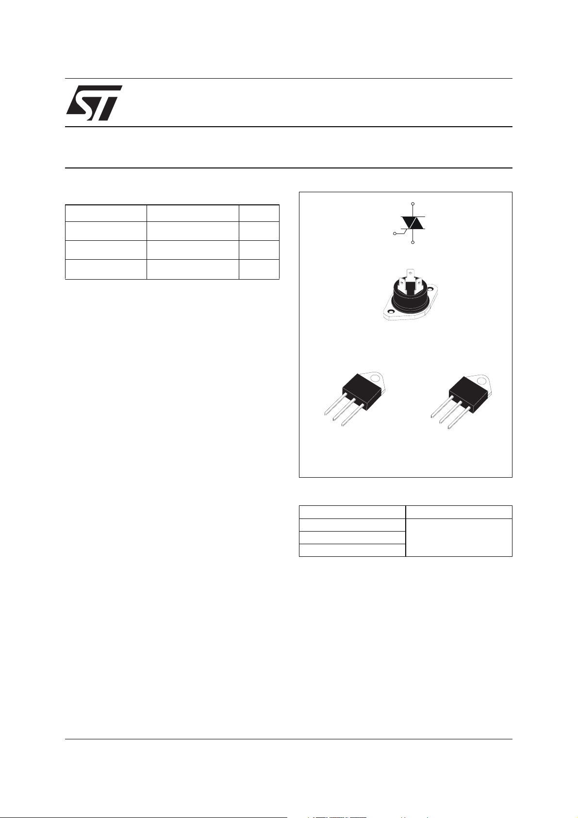
BTA40, BTA41 and BTB41 Series
STANDARD
Table 1: Main Features
Symbol Value Unit
I
T(RMS)
V
DRM/VRRM
I
GT (Q1)
40 A
600 and 800 V
50 mA
DESCRIPTION
Available in high power packages, the BTA/
BTB40-41 series is suitable for general purpose
AC switching. They can be used as an ON/OFF
function in applications such as static relays, heating regulation, induction motor starting circuits... or
for phase control operation in light dimmers, motor
speed controllers, ...
Thanks to their clip assembly technique, they
provide a superior performance in surge current
handling capabilities.
By using an internal ceramic pad, the BTA series
provides voltage insulated tab (rated at
2500V
) complying with UL standards (File ref.:
RMS
E81734).
A2
G
A1
A1
G
RD91
(BTA40)
A1
A2
G
TOP3 Insulated
(BTA41)
Table 2: Order Codes
Part Number Marking
BTA40-xxxB
See table 8 on page 6BTA41-xxxBRG
BTB41-xxxBRG
40A TRIACS
A2
A2
A1
A2
G
TOP3
(BTB41)
REV. 7October 2005
1/7

BTA40, BTA41 and BTB41 Series
Table 3: Absolute Maximum Ratings
Symbol Parameter Value Unit
T
I
T(RMS)
I
TSM
²
I
tI
dI/dt
V
DSM/VRSM
I
GM
P
G(AV)
T
stg
T
j
RMS on-state current
(full sine wave)
Non repetitive surge peak on-state
current (full cycle, T
²
t Value for fusing
initial = 25°C)
j
Critical rate of rise of on-state cur-
= 2 x IGT , tr ≤ 100 ns
rent I
G
Non repetitive surge peak off-state
voltage
Peak gate current
Average gate power dissipation
Storage junction temperature range
Operating junction temperature range
RD91 / TOP3
TOP Ins.
F = 50 Hz t = 20 ms 400
F = 60 Hz t = 16.7 ms 420
t
= 10 ms
p
F = 120 Hz
= 10 ms Tj = 25°C
t
p
t
= 20 µs Tj = 125°C
p
= 95°C
c
= 80°C
T
c
= 125°C
T
j
T
= 125°C
j
40 A
880
50 A/µs
V
DSM/VRSM
+ 100
8A
1W
- 40 to + 150
- 40 to + 125
A
°C
A
²
s
V
Tables 4: Electrical Characteristics (T
= 25°C, unless otherwise specified)
j
Symbol Test Conditions Quadrant Value Unit
I
(1)
GT
V
GT
V
GD
(2) IT = 500 mA
I
H
I
L
dV/dt (2)
V
= 12 V RL = 33 Ω
D
VD = V
IG = 1.2 I
= 67 %V
V
D
RL = 3.3 kΩ Tj = 125°C
DRM
GT
gate open Tj = 125°C
DRM
(dV/dt)c (2) (dI/dt)c = 20 A/ms
I - II - III
IV
MAX.
ALL MAX. 1.3 V
ALL MIN. 0.2 V
MAX. 80 mA
I - III - IV
MAX.
II 160
MIN. 500 V/µs
T
= 125°C
j
MIN. 10 V/µs
50
100
70
Table 5: Static Characteristics
Symbol Test Conditions Value Unit
V
(2) ITM = 60 A tp = 380 µs Tj = 25°C
T
(2)
V
t0
(2)
R
d
I
DRM
I
RRM
Note 1: minimum IGT is guaranted at 5% of IGT max.
Note 2: for both polarities of A2 referenced to A1.
Threshold voltage
Dynamic resistance
V
= V
DRM
RRM
Tj = 125°C
Tj = 125°C
Tj = 25°C
= 125°C
T
j
MAX. 1.55 V
MAX. 0.85 V
MAX. 10 mΩ
5µA
MAX.
5mA
mA
mA
2/7
BTA40, BTA41 and BTB41 Series
Table 6: Thermal resistance
Symbol Parameter Value Unit
R
R
th(j-c)
th(j-a)
Junction to case (AC)
Junction to ambient TOP3 / TOP3 Insulated 50 °C/W
S = Copper surface under tab.
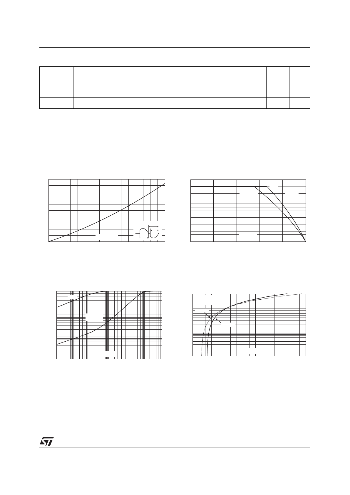
Figure 1: Maximum power dissipation versus
RMS on-state current (full cycle)
P(W)
50
40
30
20
180°
10
I (A)
0
0 5 10 15 20 25 30 35 40
T(RMS)
α
α
RD91 (Insulated) / TOP3 0.9
TOP3 Insulated 0.6
Figure 2: RMS on-state current versus case
temperature (full cycle)
I (A)
T(RMS)
45
40
35
30
25
20
15
10
5
0
0 25 50 75 100 125
BTA40 / BTB41
T (°C)
C
BTA41
°C/W
α = 180°
Figure 3: Relative variation of thermal
impedance versus pulse duration
K=[Z /R
1.E+00
1.E-01
1.E-02
1.E-03
1.E-03 1.E-02 1.E-01 1.E+00 1.E+01 1.E+02 1.E+03
th th
Z
th(j-c)
]
Z
th(j-a)
BTA / BTB41
t (s)
p
Figure 4: On-state characteristics (maximum
values)
I (A)
TM
400
100
T max.
j
V = 0.85V
to
R = 10 m
Ω
d
T=jT max.
j
T = 25°Cj.
10
V (V)
1
0.5 1.0 1.5 2.0 2.5 3.0 3.5 4.0 4.5 5.0
TM
3/7
 Loading...