

Philips bta208 DATASHEETS
Philips Semiconductors Product specification
Three quadrant triacs BTA208 series B
high commutation
GENERAL DESCRIPTION QUICK REFERENCE DATA
Glass passivated high commutation SYMBOL PARAMETER MAX. MAX. MAX. UNIT
triacsinaplasticenvelopeintendedfor
use in circuits where high static and BTA208- 500B 600B 800B
dynamic dV/dt and high dI/dt can V
DRM
occur. These devices will commutate off-state voltages
the full rated rms current at the I
maximum rated junction temperature, I
T(RMS)
TSM
without the aid of a snubber. current
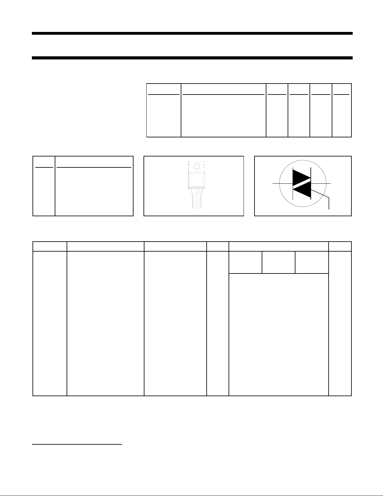
PINNING - TO220AB PIN CONFIGURATION SYMBOL
Repetitive peak 500 600 800 V
RMS on-state current 8 8 8 A
Non-repetitive peak on-state 65 65 65 A
PIN DESCRIPTION
tab
1 main terminal 1
2 main terminal 2
3 gate
tab main terminal 2
123
G
LIMITING VALUES
Limiting values in accordance with the Absolute Maximum System (IEC 134).
SYMBOL PARAMETER CONDITIONS MIN. MAX. UNIT
-500 -600 -800
V
DRM
Repetitive peak off-state - 500
1
voltages
I
T(RMS)
I
TSM
RMS on-state current full sine wave; - 8 A
Tmb ≤ 102 ˚C
Non-repetitive peak full sine wave;
on-state current Tj = 25 ˚C prior to
surge
t = 20 ms - 65 A
I2tI
2
t for fusing t = 10 ms - 21 A2s
t = 16.7 ms - 71 A
dIT/dt Repetitive rate of rise of ITM = 12 A; IG = 0.2 A; 100 A/µs
on-state current after dIG/dt = 0.2 A/µs
triggering
I
V
P
P
GM
GM
GM
G(AV)
Peak gate current - 2 A
Peak gate voltage - 5 V
Peak gate power - 5 W
Average gate power over any 20 ms - 0.5 W
period
T
stg
T
j
Storage temperature -40 150 ˚C
Operating junction - 125 ˚C
temperature
600
1
800 V
T1T2
1 Although not recommended, off-state voltages up to 800V may be applied without damage, but the triac may
switch to the on-state. The rate of rise of current should not exceed 6 A/µs.
September 1997 1 Rev 1.200

Philips Semiconductors Product specification
Three quadrant triacs BTA208 series B
high commutation
THERMAL RESISTANCES
SYMBOL PARAMETER CONDITIONS MIN. TYP. MAX. UNIT
R
th j-mb
R
th j-a
STATIC CHARACTERISTICS
Tj = 25 ˚C unless otherwise stated
SYMBOL PARAMETER CONDITIONS MIN. TYP. MAX. UNIT
I
GT
I
L
I
H
V
T
V
GT
I
D
Thermal resistance full cycle - - 2.0 K/W
junction to mounting base half cycle - - 2.4 K/W
Thermal resistance in free air - 60 - K/W
junction to ambient
Gate trigger current
2
VD = 12 V; IT = 0.1 A
T2+ G+ 2 18 50 mA
T2+ G- 2 21 50 mA
T2- G- 2 34 50 mA
Latching current VD = 12 V; IGT = 0.1 A
T2+ G+ - 31 60 mA
T2+ G- - 34 90 mA
T2- G- - 30 60 mA
Holding current VD = 12 V; IGT = 0.1 A - 31 60 mA
On-state voltage IT = 10 A - 1.3 1.65 V
Gate trigger voltage VD = 12 V; IT = 0.1 A - 0.7 1.5 V
VD = 400 V; IT = 0.1 A; Tj = 125 ˚C 0.25 0.4 - V
Off-state leakage current VD = V
; Tj = 125 ˚C - 0.1 0.5 mA
DRM(max)
DYNAMIC CHARACTERISTICS
Tj = 25 ˚C unless otherwise stated
SYMBOL PARAMETER CONDITIONS MIN. TYP. MAX. UNIT
dVD/dt Critical rate of rise of VDM = 67% V
off-state voltage exponential waveform; gate open circuit
dI
/dt Critical rate of change of VDM = 400 V; Tj = 125 ˚C; I
com
t
gt
commutating current without snubber; gate open circuit
Gate controlled turn-on ITM = 12 A; VD = V
time dIG/dt = 5 A/µs
; Tj = 125 ˚C; 1000 4000 - V/µs
DRM(max)
= 8 A; - 14 - A/ms
T(RMS)
; IG = 0.1 A; - 2 - µs
DRM(max)
2 Device does not trigger in the T2-, G+ quadrant.
September 1997 2 Rev 1.200
 Loading...