

Philips BTA204X-600F, BTA204X-600E Datasheet
Philips Semiconductors Product specification
Three quadrant triacs BTA204X series D, E and F
guaranteed commutation
GENERAL DESCRIPTION QUICK REFERENCE DATA
Passivated guaranteed commutation SYMBOL PARAMETER MAX. MAX. MAX. UNIT
triacs in a plastic full pack envelope,
intended for use in motor control BTA204X- 500D 600D -
circuits or with other highly inductive BTA204X- 500E 600E 800E
loads. These devices balance the BTA204X- 500F 600F 800F
requirements of commutation V
DRM
Repetitive peak 500 600 800 V
performance andgate sensitivity. The off-state voltages
"sensitive gate" E series and "logic I
T(RMS)
RMS on-state current 4 4 4 A
level" D series are intended for I
TSM
Non-repetitive peak on-state 25 25 25 A
interfacing with low power drivers, current
including micro controllers.
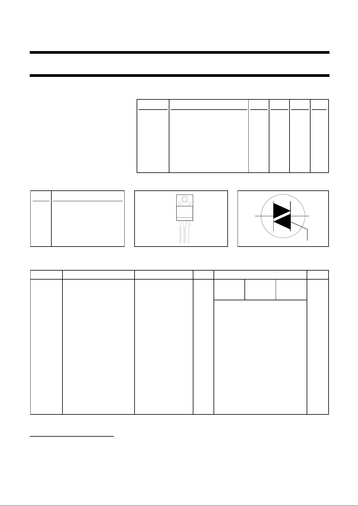
PINNING - SOT186A PIN CONFIGURATION SYMBOL
PIN DESCRIPTION
1 main terminal 1
2 main terminal 2
3 gate
case isolated
LIMITING VALUES
Limiting values in accordance with the Absolute Maximum System (IEC 134).
SYMBOL PARAMETER CONDITIONS MIN. MAX. UNIT
-500 -600 -800
V
DRM
Repetitive peak off-state - 500
1
600
1
800 V
voltages
I
T(RMS)
RMS on-state current full sine wave; - 4 A
Ths ≤ 92 ˚C
I
TSM
Non-repetitive peak full sine wave;
on-state current Tj = 25 ˚C prior to
surge
t = 20 ms - 25 A
t = 16.7 ms - 27 A
I2tI
2
t for fusing t = 10 ms - 3.1 A2s
dIT/dt Repetitive rate of rise of ITM = 6 A; IG = 0.2 A; 100 A/µs
on-state current after dIG/dt = 0.2 A/µs
triggering
I
GM
Peak gate current - 2 A
V
GM
Peak gate voltage - 5 V
P
GM
Peak gate power - 5 W
P
G(AV)
Average gate power over any 20 ms - 0.5 W
period
T
stg
Storage temperature -40 150 ˚C
T
j
Operating junction - 125 ˚C
temperature
T1T2
G
123
case
1 Although not recommended, off-state voltages up to 800V may be applied without damage, but the triac may
switch to the on-state. The rate of rise of current should not exceed 6 A/µs.
December 1998 1 Rev 1.000
Philips Semiconductors Product specification
Three quadrant triacs BTA204X series D, E and F
guaranteed commutation
ISOLATION LIMITING VALUE & CHARACTERISTIC
Ths = 25 ˚C unless otherwise specified
SYMBOL PARAMETER CONDITIONS MIN. TYP. MAX. UNIT
V
isol
R.M.S. isolation voltage from all f = 50-60 Hz; sinusoidal - 2500 V
three terminals to external waveform;
heatsink R.H. ≤ 65% ; clean and dustfree
C
isol
Capacitance from T2 to external f = 1 MHz - 10 - pF
heatsink
THERMAL RESISTANCES
SYMBOL PARAMETER CONDITIONS MIN. TYP. MAX. UNIT
R
th j-hs
Thermal resistance full or half cycle
junction to heatsink with heatsink compound - - 5.5 K/W
without heatsink compound - - 7.2 K/W
R
th j-a
Thermal resistance in free air - 55 - K/W
junction to ambient
STATIC CHARACTERISTICS
Tj = 25 ˚C unless otherwise stated
SYMBOL PARAMETER CONDITIONS MIN. TYP. MAX. UNIT
BTA204X- ...D ...E ...F
I
GT
Gate trigger current
2
VD = 12 V; IT = 0.1 A
T2+ G+ - - 5 10 25 mA
T2+ G- - - 5 10 25 mA
T2- G- - - 5 10 25 mA
I
L
Latching current VD = 12 V; IGT = 0.1 A
T2+ G+ - - 6 12 20 mA
T2+ G- - - 9 18 30 mA
T2- G- - - 6 12 20 mA
I
H
Holding current VD = 12 V; IGT = 0.1 A - - 6 12 20 mA
V
T
On-state voltage IT = 5 A - 1.4 1.7 V
V
GT
Gate trigger voltage VD = 12 V; IT = 0.1 A - 0.7 1.5 V
VD = 400 V; IT = 0.1 A; 0.25 0.4 - V
Tj = 125 ˚C
I
D
Off-state leakage current VD = V
DRM(max)
; - 0.1 0.5 mA
Tj = 125 ˚C
2 Device does not trigger in the T2-, G+ quadrant.
December 1998 2 Rev 1.000

Philips Semiconductors Product specification
Three quadrant triacs BTA204X series D, E and F
guaranteed commutation
DYNAMIC CHARACTERISTICS
Tj = 25 ˚C unless otherwise stated
SYMBOL PARAMETER CONDITIONS MIN. TYP. MAX. UNIT
BTA204X- ...D ...E ...F
dVD/dt Critical rate of rise of VDM = 67% V
DRM(max)
;20 3050- -V/µs
off-state voltage Tj = 125 ˚C; exponential
waveform; gate open
circuit
dI
com
/dt Critical rate of change of VDM = 400 V; Tj = 125 ˚C; 1.0 2.0 2.5 - - A/ms
commutating current I
T(RMS)
= 4 A;
dV
com
/dt = 20V/µs; gate
open circuit
dI
com
/dt Critical rate of change of VDM = 400 V; Tj = 125 ˚C; 5.0 - - - - A/ms
commutating current I
T(RMS)
= 4 A;
dV
com
/dt = 0.1V/µs; gate
open circuit
t
gt
Gate controlled turn-on ITM = 12 A; VD = V
DRM(max)
;- - - 2 - µs
time IG = 0.1 A; dIG/dt = 5 A/µs
December 1998 3 Rev 1.000
 Loading...