


Philips Semiconductors Product specification
Thyristor BT169W Series
logic level
GENERAL DESCRIPTION QUICK REFERENCE DATA
Glass passivated, sensitive gate SYMBOL PARAMETER MAX. MAX. MAX. MAX. UNIT
thyristorinaplasticenvelope,suitable
forsurfacemounting,intended foruse BT169 BW DW EW GW
in general purpose switching and V
DRM
, Repetitive peak 200 400 500 600 V
phase control applications. This V
RRM
off-state voltages
device is intended to be interfaced I
T(AV)
Average on-state 0.5 0.5 0.5 0.5 A
directly to microcontrollers, logic current
integrated circuits and other low I
T(RMS)
RMS on-state current 0.8 0.8 0.8 0.8 A
power gate trigger circuits. I
TSM
Non-repetitive peak 8888A
on-state current
PINNING - SOT223 PIN CONFIGURATION SYMBOL
PIN DESCRIPTION
1 cathode
2 anode
3 gate
tab anode
LIMITING VALUES
Limiting values in accordance with the Absolute Maximum System (IEC 134).
SYMBOL PARAMETER CONDITIONS MIN. MAX. UNIT
BDEG
V
DRM
, V
RRM
Repetitive peak off-state - 200140015001600
1
V
voltages
I
T(AV)
Average on-state current half sine wave; - 0.63 A
Tsp ≤ 112 ˚C
I
T(RMS)
RMS on-state current all conduction angles - 1 A
I
TSM
Non-repetitive peak half sine wave;
on-state current Tj = 25 ˚C prior to surge
t = 10 ms - 8 A
t = 8.3 ms - 9 A
I2tI
2
t for fusing t = 10 ms - 0.32 A2s
dIT/dt Repetitive rate of rise of ITM = 2 A; IG = 10 mA; - 50 A/µs
on-state current after dIG/dt = 100 mA/µs
triggering
I
GM
Peak gate current - 1 A
V
GM
Peak gate voltage - 5 V
V
RGM
Peak reverse gate voltage - 5 V
P
GM
Peak gate power - 2 W
P
G(AV)
Average gate power over any 20 ms period - 0.1 W
T
stg
Storage temperature -40 150 ˚C
T
j
Operating junction - 125 ˚C
temperature
ak
g
4
1
23
1 Although not recommended, off-state voltages up to 800V may be applied without damage, but the thyristor may
switch to the on-state. The rate of rise of current should not exceed 15 A/µs.
September 1997 1 Rev 1.200

Philips Semiconductors Product specification
Thyristor BT169W Series
logic level
THERMAL RESISTANCES
SYMBOL PARAMETER CONDITIONS MIN. TYP. MAX. UNIT
R
th j-sp
Thermal resistance - - 15 K/W
junction to solder point
R
th j-a
Thermal resistance pcb mounted, minimum footprint - 156 - K/W
junction to ambient pcb mounted; pad area as in fig:14 - 70 - K/W
STATIC CHARACTERISTICS
Tj = 25 ˚C unless otherwise stated
SYMBOL PARAMETER CONDITIONS MIN. TYP. MAX. UNIT
I
GT
Gate trigger current VD = 12 V; IT = 10 mA; gate open circuit - 50 200 µA
I
L
Latching current VD = 12 V; IGT = 0.5 mA; RGK = 1 kΩ -26mA
I
H
Holding current VD = 12 V; IGT = 0.5 mA; RGK = 1 kΩ -25mA
V
T
On-state voltage IT = 2 A - 1.35 1.5 V
V
GT
Gate trigger voltage VD = 12 V; IT = 10 mA; gate open circuit - 0.5 0.8 V
VD = V
DRM(max)
; IT = 10 mA; Tj = 125 ˚C; 0.2 0.3 - V
gate open circuit
ID, I
R
Off-state leakage current VD = V
DRM(max)
; VR = V
RRM(max)
; Tj = 125 ˚C; - 0.05 0.1 mA
RGK = 1 kΩ
DYNAMIC CHARACTERISTICS
Tj = 25 ˚C unless otherwise stated
SYMBOL PARAMETER CONDITIONS MIN. TYP. MAX. UNIT
dVD/dt Critical rate of rise of VDM =67% V
DRM(max)
; Tj = 125 ˚C; - 25 - V/µs
off-state voltage exponential waveform; RGK = 1k Ω
t
gt
Gate controlled turn-on ITM = 2 A; VD = V
DRM(max)
; IG = 10 mA; - 2 - µs
time dIG/dt = 0.1 A/µs
t
q
Circuit commutated VD = 67% V
DRM(max)
; Tj = 125 ˚C; - 100 - µs
turn-off time ITM = 1.6 A; VR = 35 V; dITM/dt = 30 A/µs;
dVD/dt = 2 V/µs; RGK = 1 kΩ
September 1997 2 Rev 1.200
Philips Semiconductors Product specification
Thyristor BT169W Series
logic level
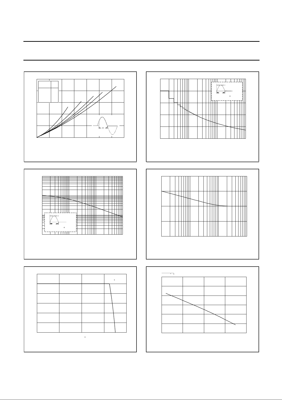
Fig.1. Maximum on-state dissipation, P
tot
, versus
average on-state current, I
T(AV)
, where a = form
factor = I
T(RMS)
/ I
T(AV)
.
Fig.2. Maximum permissible non-repetitive peak
on-state current I
TSM
, versus pulse width tp, for
sinusoidal currents, tp ≤ 10ms.
Fig.3. Maximum permissible rms current I
T(RMS)
,
versus solder point temperature Tsp.
Fig.4. Maximum permissible non-repetitive peak
on-state current I
TSM
, versus number of cycles, for
sinusoidal currents, f = 50 Hz.
Fig.5. Maximum permissible repetitive rms on-state
current I
T(RMS)
, versus surge duration, for sinusoidal
currents, f = 50 Hz; Tsp ≤ 112˚C.
Fig.6. Normalised gate trigger voltage
VGT(Tj)/ VGT(25˚C), versus junction temperature Tj.
0 0.1 0.2 0.3 0.4 0.5 0.6 0.7
0
0.2
0.4
0.6
0.8
1
a = 1.57
1.9
2.2
2.8
4
BT169W
IF(AV) / A
Ptot / W
125
122
119
116
113
110
Tsp(max) / C
conduction
angle
form
factor
degrees
30
60
90
120
180
4
2.8
2.2
1.9
1.57
a
1 10 100 1000
0
2
4
6
8
10
BT169
Number of half cycles at 50Hz
ITSM / A
T
I
TSM
time
I
Tj initial = 25 C max
T
1
10
100
1000
BT169
10us 100us 1ms
10ms
T / s
ITSM / A
T
I
TSM
time
I
Tj initial = 25 C max
T
0.01 0.1 1 10
0
0.5
1
1.5
2
BT134W
surge duration / s
IT(RMS) / A
-50 0 50 100 150
0
0.2
0.4
0.6
0.8
1
1.2
BT134W
Tsp / C
IT(RMS) / A
112 C
-50 0 50 100 150
0.4
0.6
0.8
1
1.2
1.4
1.6
BT151
Tj / C
VGT(Tj)
VGT(25 C)
September 1997 3 Rev 1.200
 Loading...