

Philips bt151x DATASHEETS
Philips Semiconductors Product specification
Thyristors BT151X series
GENERAL DESCRIPTION QUICK REFERENCE DATA
Passivated thyristors in a full pack, SYMBOL PARAMETER MAX. MAX. MAX. UNIT
plastic envelope, intended for use in
applications requiring high BT151X- 500 650 800
bidirectional blocking voltage V
capability and high thermal cycling V
performance. Typical applications I
include motor control, industrial and I
domestic lighting, heating and static I
switching. current
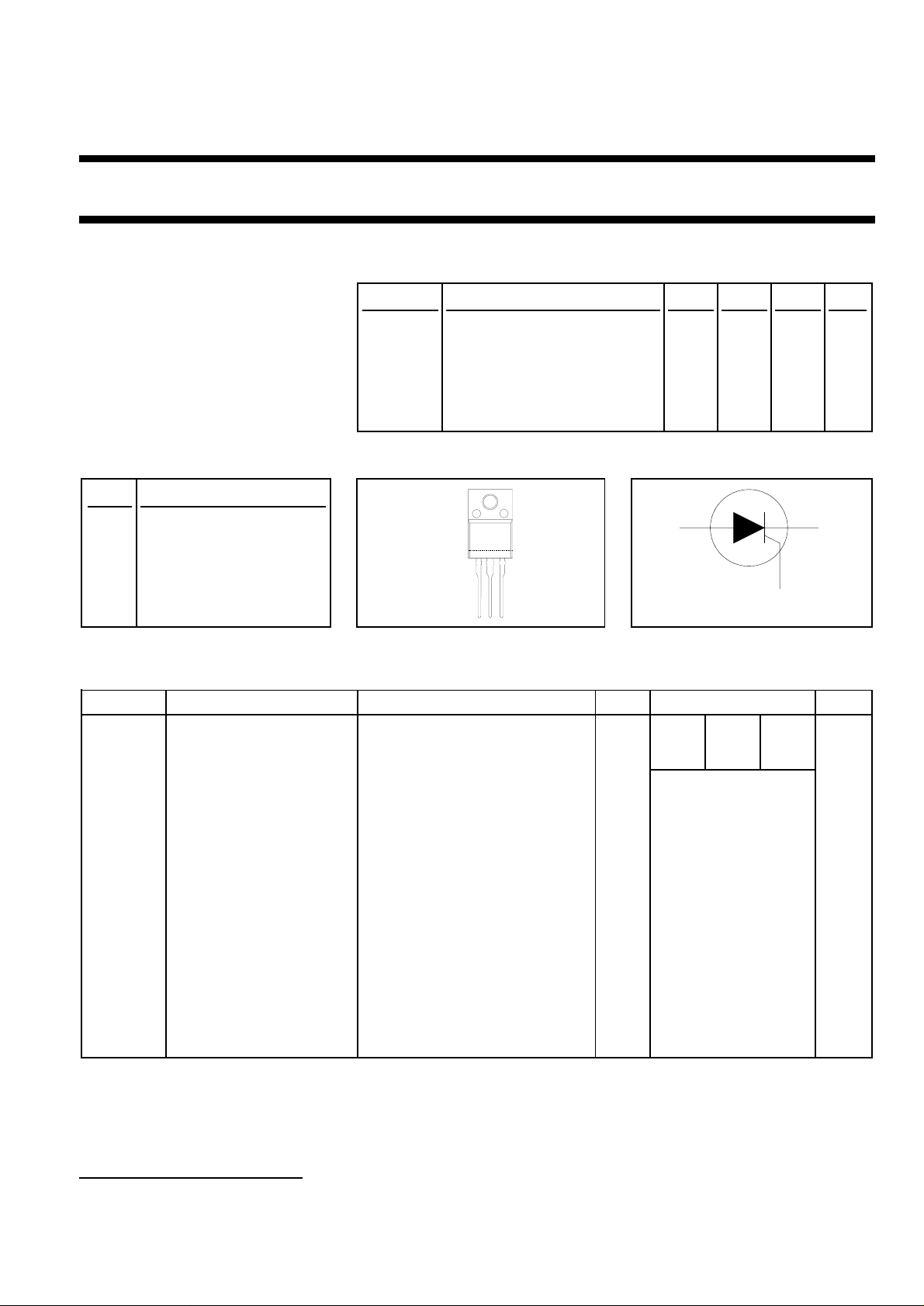
PINNING - SOT186A PIN CONFIGURATION SYMBOL
, Repetitive peak off-state 500 650 800 V
DRM
RRM
T(AV)
T(RMS)
TSM
voltages
Average on-state current 5.7 5.7 5.7 A
RMS on-state current 9 9 9 A
Non-repetitive peak on-state 100 100 100 A
PIN DESCRIPTION
1 cathode
case
ak
2 anode
3 gate
case isolated
123
g
LIMITING VALUES
Limiting values in accordance with the Absolute Maximum System (IEC 134).
SYMBOL PARAMETER CONDITIONS MIN. MAX. UNIT
-500 -650 -800
V
DRM
I
T(AV)
I
T(RMS)
I
TSM
, V
Repetitive peak off-state - 5001650
RRM
voltages
Average on-state current half sine wave; Ths ≤ 87 ˚C - 5.7 A
RMS on-state current all conduction angles - 9 A
Non-repetitive peak half sine wave; Tj = 25 ˚C prior to
on-state current surge
t = 10 ms - 100 A
I2tI
2
t for fusing t = 10 ms - 50 A2s
t = 8.3 ms - 110 A
dIT/dt Repetitive rate of rise of ITM = 20 A; IG = 50 mA; - 50 A/µs
on-state current after dIG/dt = 50 mA/µs
triggering
I
V
V
P
P
T
T
GM
GM
RGM
GM
G(AV)
stg
j
Peak gate current - 2 A
Peak gate voltage - 5 V
Peak reverse gate voltage - 5 V
Peak gate power - 5 W
Average gate power over any 20 ms period - 0.5 W
Storage temperature -40 150 ˚C
Operating junction - 125 ˚C
temperature
1
800 V
1 Although not recommended, off-state voltages up to 800V may be applied without damage, but the thyristor may
switch to the on-state. The rate of rise of current should not exceed 15 A/µs.
June 1999 1 Rev 1.300

Philips Semiconductors Product specification
Thyristors BT151X series
ISOLATION LIMITING VALUE & CHARACTERISTIC
Ths = 25 ˚C unless otherwise specified
SYMBOL PARAMETER CONDITIONS MIN. TYP. MAX. UNIT
V
isol
C
isol
THERMAL RESISTANCES
SYMBOL PARAMETER CONDITIONS MIN. TYP. MAX. UNIT
R
th j-hs
R
th j-a
STATIC CHARACTERISTICS
Tj = 25 ˚C unless otherwise stated
SYMBOL PARAMETER CONDITIONS MIN. TYP. MAX. UNIT
I
GT
I
L
I
H
V
T
V
GT
ID, I
R
R.M.S. isolation voltage from all f = 50-60 Hz; sinusoidal - 2500 V
three terminals to external waveform;
heatsink R.H. ≤ 65% ; clean and dustfree
Capacitance from T2 to external f = 1 MHz - 10 - pF
heatsink
Thermal resistance with heatsink compound - - 4.5 K/W
junction to heatsink without heatsink compound - - 6.5 K/W
Thermal resistance in free air - 55 - K/W
junction to ambient
Gate trigger current VD = 12 V; IT = 0.1 A - 2 15 mA
Latching current VD = 12 V; IGT = 0.1 A - 10 40 mA
Holding current VD = 12 V; IGT = 0.1 A - 7 20 mA
On-state voltage IT = 23 A - 1.4 1.75 V
Gate trigger voltage VD = 12 V; IT = 0.1 A - 0.6 1.5 V
Off-state leakage current VD = V
VD = V
; IT = 0.1 A; Tj = 125 ˚C 0.25 0.4 - V
DRM(max)
DRM(max)
; VR = V
; Tj = 125 ˚C - 0.1 0.5 mA
RRM(max)
DYNAMIC CHARACTERISTICS
Tj = 25 ˚C unless otherwise stated
SYMBOL PARAMETER CONDITIONS MIN. TYP. MAX. UNIT
dVD/dt Critical rate of rise of VDM = 67% V
off-state voltage exponential waveform
t
gt
Gate controlled turn-on ITM = 40 A; VD = V
time dIG/dt = 5 A/µs
t
q
Circuit commutated VD = 67% V
turn-off time ITM = 20 A; VR = 25 V; dITM/dt = 30 A/µs;
dVD/dt = 50 V/µs; RGK = 100 Ω
DRM(max)
; Tj = 125 ˚C;
DRM(max)
Gate open circuit 50 130 - V/µs
RGK = 100 Ω 200 1000 - V/µs
; IG = 0.1 A; - 2 - µs
DRM(max)
; Tj = 125 ˚C; - 70 - µs
June 1999 2 Rev 1.300
 Loading...