

Philips BT136B D Technical data
查询BT136B-500D供应商
Philips Semiconductors Product specification
Triacs BT136B series D
logic level
GENERAL DESCRIPTION QUICK REFERENCE DATA
Glass passivated, sensitive gate SYMBOL PARAMETER MAX. MAX. UNIT
triacsinaplastic envelopesuitablefor
surface mounting, intended for use in BT136B- 500D 600D
general purpose bidirectional V
switching and phase control I
applications. These devices are I
intended to be interfaced directly to
DRM
T(RMS)
TSM
microcontrollers, logic integrated
circuits and other low power gate
trigger circuits.
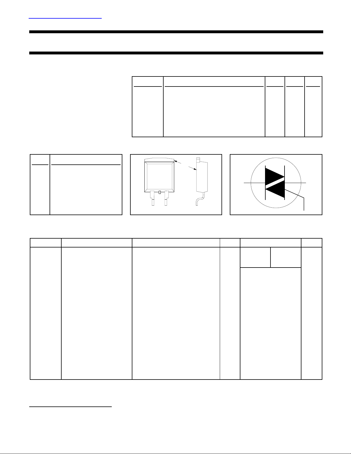
PINNING - SOT404 PIN CONFIGURATION SYMBOL
Repetitive peak off-state voltages 500 600 V
RMS on-state current 4 4 A
Non-repetitive peak on-state current 25 25 A
PIN DESCRIPTION
mb
1 main terminal 1
2 main terminal 2
3 gate
mb main terminal 2
2
13
LIMITING VALUES
Limiting values in accordance with the Absolute Maximum System (IEC 134).
SYMBOL PARAMETER CONDITIONS MIN. MAX. UNIT
-500 -600
V
DRM
Repetitive peak off-state - 500
voltages
I
T(RMS)
I
TSM
RMS on-state current full sine wave; Tmb ≤ 107 ˚C - 4 A
Non-repetitive peak full sine wave; Tj = 25 ˚C prior to
on-state current surge
t = 20 ms - 25 A
I2tI
2
t for fusing t = 10 ms - 3.1 A2s
t = 16.7 ms - 27 A
dIT/dt Repetitive rate of rise of ITM = 6 A; IG = 0.2 A;
on-state current after dIG/dt = 0.2 A/µs
triggering T2+ G+ - 50 A/µs
I
V
P
P
T
T
GM
GM
GM
G(AV)
stg
j
Peak gate current - 2 A
Peak gate voltage - 5 V
Peak gate power - 5 W
Average gate power over any 20 ms period - 0.5 W
Storage temperature -40 150 ˚C
Operating junction - 125 ˚C
temperature
1
T2+ G- - 50 A/µs
T2- G- - 50 A/µs
T2- G+ - 10 A/µs
600
1
T1T2
G
V
1 Although not recommended, off-state voltages up to 800V may be applied without damage, but the triac may
switch to the on-state. The rate of rise of current should not exceed 3 A/µs.
October 1997 1 Rev 1.100

Philips Semiconductors Product specification
Triacs BT136B series D
logic level
THERMAL RESISTANCES
SYMBOL PARAMETER CONDITIONS MIN. TYP. MAX. UNIT
R
th j-mb
R
th j-a
STATIC CHARACTERISTICS
Tj = 25 ˚C unless otherwise stated
SYMBOL PARAMETER CONDITIONS MIN. TYP. MAX. UNIT
I
GT
I
L
I
H
V
T
V
GT
I
D
Thermal resistance full cycle - - 3.0 K/W
junction to mounting base half cycle - - 3.7 K/W
Thermal resistance minimum footprint, FR4 board - 55 - K/W
junction to ambient
Gate trigger current VD = 12 V; IT = 0.1 A
T2+ G+ - 2.0 5 mA
T2+ G- - 2.5 5 mA
T2- G- - 2.5 5 mA
T2- G+ - 5.0 10 mA
Latching current VD = 12 V; IGT = 0.1 A
T2+ G+ - 1.6 10 mA
T2+ G- - 4.5 15 mA
T2- G- - 1.2 10 mA
T2- G+ - 2.2 15 mA
Holding current VD = 12 V; IGT = 0.1 A - 1.2 10 mA
On-state voltage IT = 5 A - 1.4 1.70 V
Gate trigger voltage VD = 12 V; IT = 0.1 A - 0.7 1.5 V
VD = 400 V; IT = 0.1 A; Tj = 125 ˚C 0.25 0.4 - V
Off-state leakage current VD = V
; Tj = 125 ˚C - 0.1 0.5 mA
DRM(max)
DYNAMIC CHARACTERISTICS
Tj = 25 ˚C unless otherwise stated
SYMBOL PARAMETER CONDITIONS MIN. TYP. MAX. UNIT
dVD/dt Critical rate of rise of VDM = 67% V
off-state voltage exponential waveform; RGK = 1 kΩ
t
gt
Gate controlled turn-on ITM = 6 A; VD = V
time dIG/dt = 5 A/µs
; Tj = 125 ˚C; - 5 - V/µs
DRM(max)
; IG = 0.1 A; - 2 - µs
DRM(max)
October 1997 2 Rev 1.100
 Loading...