

Philips BSX63, BSX62 Datasheet

DISCRETE SEMICONDUCTORS
DATA SH EET
M3D111
BSX62; BSX63
NPN switching transistors
Product specification
Supersedes data of September 1994
File under Discrete Semiconductors, SC04
1997 Jun 19
Philips Semiconductors Product specification
NPN switching transistors BSX62; BSX63
FEATURES
• High current (max. 3 A)
• Low voltage (max. 60 V).
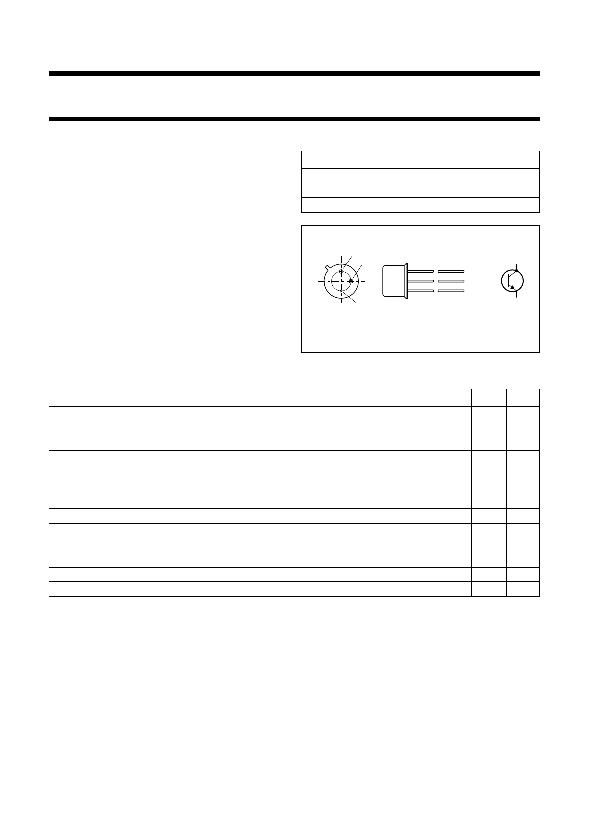
PINNING
PIN DESCRIPTION
1 emitter
2 base
APPLICATIONS
3 collector, connected to case
• Medium power switching.
DESCRIPTION
NPN switching transistor in a TO-39 metal package.
handbook, halfpage
1
2
3
MAM317
3
2
1
Fig.1 Simplified outline (TO-39) and symbol.
QUICK REFERENCE DATA
SYMBOL PARAMETER CONDITIONS MIN. TYP. MAX. UNIT
V
CBO
collector-base voltage open emitter
BSX62 −−60 V
BSX63 −−80 V
V
CEO
collector-emitter voltage open base
BSX62 −−40 V
BSX63 −−60 V
I
C
P
tot
h
FE
collector current (DC) −−3A
total power dissipation T
≤ 25 °C −−5W
case
DC current gain IC= 1 A; VCE=1V
BSX62-10; BSX63-10 63 100 160
BSX62-16; BSX63-16 100 160 250
f
T
t
off
transition frequency IC= 200 mA; VCE= 10 V; f = 100 MHz 30 70 − MHz
turn-off time I
Con
= 1 A; I
= 50 mA; I
Bon
= −50 mA −−1.5 µs
Boff
1997 Jun 19 2
Philips Semiconductors Product specification
NPN switching transistors BSX62; BSX63
LIMITING VALUES
In accordance with the Absolute Maximum Rating System (IEC 134).
SYMBOL PARAMETER CONDITIONS MIN. MAX. UNIT
V
CBO
V
CEO
V
EBO
I
C
I
CM
I
BM
P
tot
T
stg
T
j
T
amb
collector-base voltage open emitter
BSX62 − 60 V
BSX63 − 80 V
collector-emitter voltage open base
BSX62 − 40 V
BSX63 − 60 V
emitter-base voltage open collector − 5V
collector current (DC) − 3A
peak collector current − 3A
peak base current − 500 mA
total power dissipation T
≤ 25 °C − 5W
case
storage temperature −65 +150 °C
junction temperature − 200 °C
operating ambient temperature −65 +150 °C
THERMAL CHARACTERISTICS
SYMBOL PARAMETER CONDITIONS VALUE UNIT
R
R
th j-a
th j-c
thermal resistance from junction to ambient in free air 200 K/W
thermal resistance from junction to case 28 K/W
1997 Jun 19 3
 Loading...