

Philips bsx32 DATASHEETS
DISCRETE SEMICONDUCTORS
DATA SH EET
M3D111
BSX32
NPN switching transistor
Product specification
Supersedes data of September 1994
File under Discrete Semiconductors, SC04
1997 May 28

Philips Semiconductors Product specification
NPN switching transistor BSX32
FEATURES
• High current (max. 1 A)
• Low voltage (max. 40 V).
PINNING
PIN DESCRIPTION
1 emitter
2 base
APPLICATIONS
3 collector, connected to case
• High-current switching in industrial applications.
DESCRIPTION
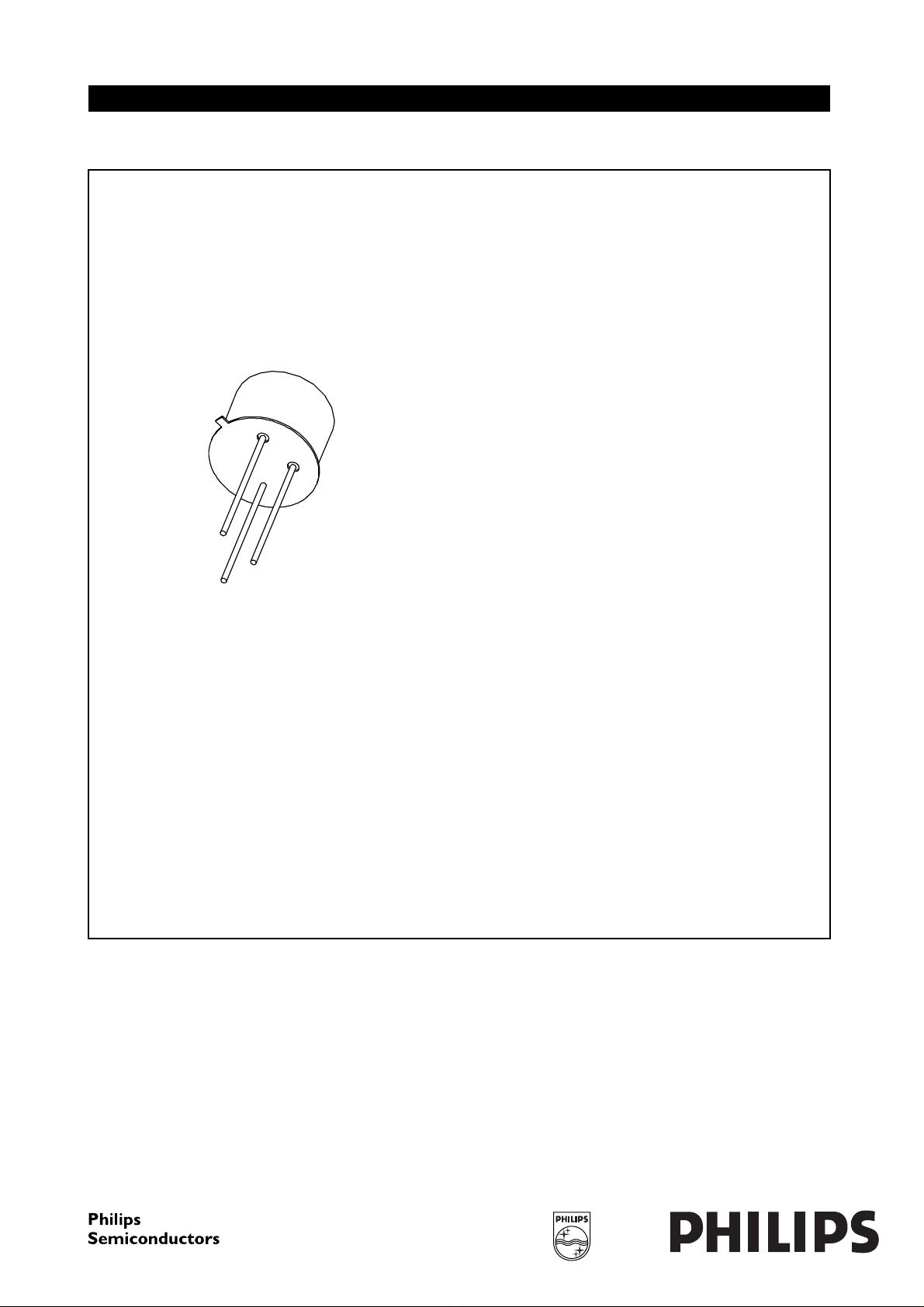
handbook, halfpage
1
2
3
NPN switching transistor in a TO-39 metal package.
2
3
MAM317
1
Fig.1 Simplified outline (TO-39) and symbol.
QUICK REFERENCE DATA
SYMBOL PARAMETER CONDITIONS MIN. TYP. MAX. UNIT
V
CBO
V
CEO
I
C
P
tot
h
FE
f
T
t
off
collector-base voltage open emitter −−65 V
collector-emitter voltage open base −−40 V
collector current (DC) −−1A
total power dissipation T
≤ 25 °C −−800 mW
amb
DC current gain IC= 1 A; VCE=5V 20 60 −
transition frequency IC= 50 mA; VCE= 10 V; f = 100 MHz 300 −−MHz
turn-off time I
= 500 mA; I
Con
= 50 mA; I
Bon
= −50 mA −−60 ns
Boff
1997 May 28 2

Philips Semiconductors Product specification
NPN switching transistor BSX32
LIMITING VALUES
In accordance with the Absolute Maximum Rating System (IEC 134).
SYMBOL PARAMETER CONDITIONS MIN. MAX. UNIT
V
CBO
V
CEO
V
EBO
I
C
I
CM
I
BM
P
tot
T
stg
T
j
T
amb
collector-base voltage open emitter − 65 V
collector-emitter voltage open base − 40 V
emitter-base voltage open collector − 6V
collector current (DC) − 1A
peak collector current − 1A
peak base current − 200 mA
total power dissipation T
≤ 25 °C − 800 mW
amb
T
≤ 25 °C − 3.5 W
case
storage temperature −65 +150 °C
junction temperature − 200 °C
operating ambient temperature −65 +150 °C
THERMAL CHARACTERISTICS
SYMBOL PARAMETER CONDITIONS VALUE UNIT
R
R
th j-a
th j-c
thermal resistance from junction to ambient in free air 219 K/W
thermal resistance from junction to case 50 K/W
1997 May 28 3
 Loading...