

Philips bst39 40 DATASHEETS
DISCRETE SEMICONDUCTORS
DATA SH EET
ook, halfpage
M3D109
BST39; BST40
NPN high-voltage transistors
Product specification
Supersedes data of 1999 Apr 26
2000 Jul 03
Philips Semiconductors Product specification
NPN high-voltage transistors BST39; BST40
FEATURES
• Low current (max. 100 mA)
• High voltage (max. 350 V).
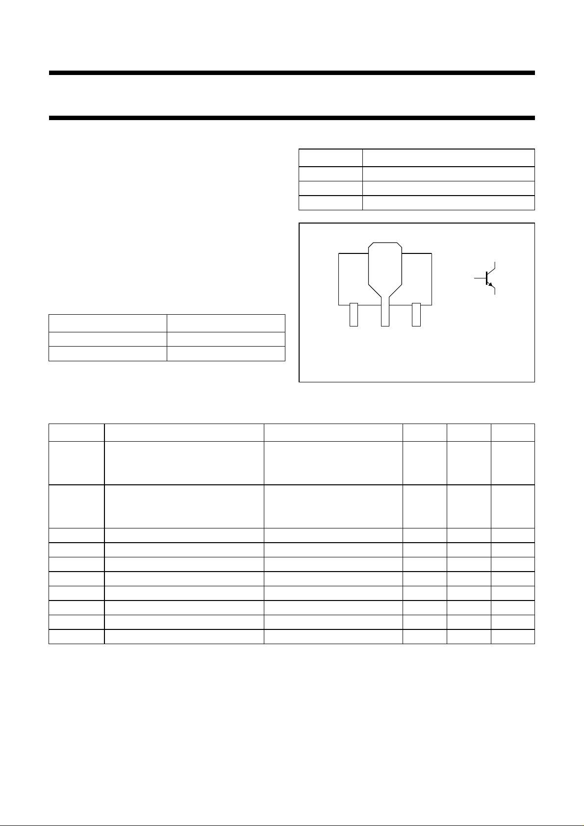
PINNING
PIN DESCRIPTION
1 emitter
2 collector
APPLICATIONS
3 base
• General purpose switching and amplification.
DESCRIPTION
handbook, halfpage
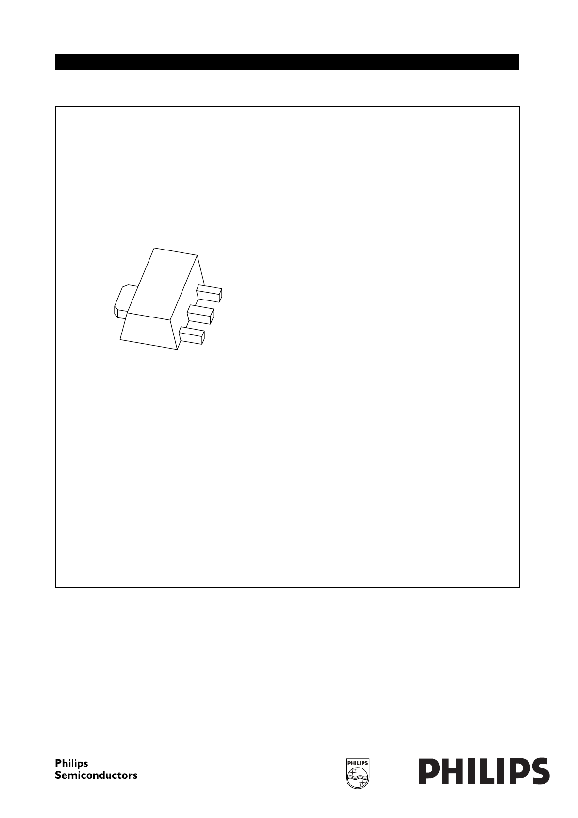
NPN high-voltage transistor in a SOT89 plastic package.
PNP complements: BST15 and BST16.
MARKING
TYPE NUMBER MARKING CODE
BST39 AT1
BST40 AT2
Fig.1 Simplified outline (SOT89) and symbol.
LIMITING VALUES
In accordance with the Absolute Maximum Rating System (IEC 60134).
123
Bottom view
2
3
1
MAM296
SYMBOL PARAMETER CONDITIONS MIN. MAX. UNIT
V
CBO
collector-base voltage open emitter
BST39 − 400 V
BST40 − 300 V
V
CEO
collector-emitter voltage open base
BST39 − 350 V
BST40 − 250 V
V
EBO
I
C
I
CM
I
BM
P
tot
T
stg
T
j
T
amb
emitter-base voltage open collector − 5V
collector current (DC) − 100 mA
peak collector current − 200 mA
peak base current − 100 mA
total power dissipation T
≤ 25 °C; note 1 − 1.3 W
amb
storage temperature −65 +150 °C
junction temperature − 150 °C
operating ambient temperature −65 +150 °C
Note
1. Device mounted on a printed-circuit board, single-sided copper, tinplated, mounting pad for collector 6 cm
For other mounting conditions,see
“Thermal considerations for SOT89 in theGeneral Partof associatedHandbook”.
2
.
2000 Jul 03 2
Philips Semiconductors Product specification
NPN high-voltage transistors BST39; BST40
THERMAL CHARACTERISTICS
SYMBOL PARAMETER CONDITIONS VALUE UNIT
R
th j-a
R
th j-s
Note
1. Device mounted on a printed-circuit board, single-sided copper, tinplated, mounting pad for collector 6 cm2.
For other mounting conditions, see
CHARACTERISTICS
Tj=25°C unless otherwise specified.
SYMBOL PARAMETER CONDITIONS MIN. MAX. UNIT
I
CBO
I
EBO
h
FE
V
CEsat
C
c
f
T
thermal resistance from junction to ambient note1 96 K/W
thermal resistance from junction to soldering point 16 K/W
“Thermal considerations for SOT89 in theGeneral Partof associatedHandbook”.
collector cut-off current IE= 0; VCB= 300 V − 20 nA
emitter cut-off current IC= 0; VEB=5V − 100 nA
DC current gain IC= 20 mA; VCE=10V 40 −
collector-emitter saturation voltage IC= 50 mA; IB=4mA − 500 mV
collector capacitance IE=ie= 0; VCB= 10 V; f = 1 MHz − 2pF
transition frequency IC= 10 mA; VCE= 10 V; f = 100 MHz 70 − MHz
2000 Jul 03 3
 Loading...