

Philips BST100 Datasheet

DISCRETE SEMICONDUCTORS
DATA SH EET
BST100
P-channel enhancement mode
vertical D-MOS transistor
Product specification
File under Discrete Semiconductors, SC13b
April 1995
Philips Semiconductors Product specification
P-channel enhancement mode vertical
D-MOS transistor
DESCRIPTION
P-channel vertical D-MOS transistor
TO-92 variant envelope and intended
for use in relay, high-speed and
line-transformer drivers.
FEATURES
• Very low R
DS(on)
• Direct interface to C-MOS
• High-speed switching
• No second breakdown
QUICK REFERENCE DATA
Drain-source voltage −V
Gate-source voltage (open drain) ±V
Drain current (DC) −I
Total power dissipation up to T
Drain-source ON-resistance
−ID= 200 mA; −VGS= 10 V R
Transfer admittance
−I
= 200 mA; −VDS= 15 V Yfs typ. 200 mS
D
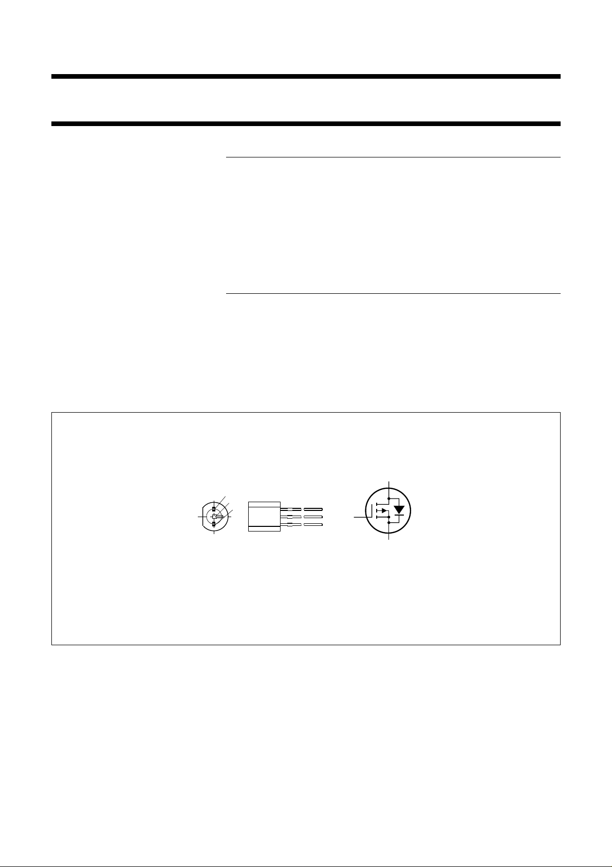
PINNING - TO-92 VARIANT
1 = source
2 = gate
3 = drain
=25°CP
amb
DS
GSO
D
tot
DS(on)
BST100
max. 60 V
max. 20 V
max. 0.3 A
max. 1 W
typ.
max.
4,56Ω
Ω
PIN CONFIGURATION
Note: various pinout configurations available.
handbook, halfpage
1
2
Fig.1 Simplified outline and symbol.
d
3
MAM144
g
s
April 1995 2

Philips Semiconductors Product specification
P-channel enhancement mode vertical
D-MOS transistor
RATINGS
Limiting values in accordance with the Absolute Maximum System (IEC 134)
Drain-source voltage −V
Gate-source voltage (open drain)
Drain current (DC) −I
Drain current (peak) −I
Total power dissipation up to T
= 25 °C (note 1) P
amb
Storage temperature range T
Junction temperature T
DS
±VGSO
D
DM
tot
stg
j
THERMAL RESISTANCE
From junction to ambient (note 1) R
th j-a
Note
1. Transistor mounted on printed-circuit board, max. lead length 4 mm, mounting pad for drain lead
min. 10 mm x 10 mm.
max. 60 V
max. 20 V
max. 0.3 A
max. 0.8 A
max. 1 W
−65 to + 150 °C
max. 150 °C
= 125 K/W
BST100
April 1995 3

Philips Semiconductors Product specification
P-channel enhancement mode vertical
D-MOS transistor
CHARACTERISTICS
T
=25°C unless otherwise specified
j
Drain-source breakdown voltage
−I
=10µA; VGS=0 −V
D
(BR)DSS
Drain-source leakage current
−VDS= 48 V; VGS=0 −I
DSS
Gate-source leakage current
−VGS= 20 V; VDS=0 −I
GSS
Gate threshold voltage
−ID= 1 mA; VDS=V
GS
−V
GS(th)
Drain-source ON-resistance
= 200 mA; −VGS= 10 V R
−I
D
DS(on)
Transfer admittance
−I
= 200 mA; −VDS= 15 V Yfs typ. 200 mS
D
Input capacitance at f = 1 MHz
−V
= 10 V; VGS=0 C
DS
iss
min. 60 V
max. 1 µA
max. 100 nA
min.
max.
typ.
max.
typ.
max.
BST100
1.5
3.5VV
4.56Ω
Ω
5570pF
pF
Output capacitance at f = 1 MHz
= 10 V; VGS=0 C
−V
DS
Feedback capacitance at f = 1 MHz
= 10 V; VGS= 0 C
−V
DS
Switching times (see Figs 2 and 3)
−ID= 200 mA; −VDD= 50 V; −VGS= 0 to 10 V
oss
rss
t
on
t
off
typ.
max.
typ.
max.
typ.
typ.
3045pF
pF
812pF
pF
420ns
ns
April 1995 4
 Loading...