

Philips BSS87 Datasheet

DISCRETE SEMICONDUCTORS
DATA SH EET
BSS87
N-channel enhancement mode
vertical D-MOS transistor
Product specification
File under Discrete Semiconductors, SC13b
April 1995
Philips Semiconductors Product specification
N-channel enhancement mode vertical
D-MOS transistor
DESCRIPTION
N-channel vertical D-MOS transistor
in a SOT89 envelope. Designed
primarily as a line current interrupter
in telephone sets, it can also be
applied in other applications such as
in relays, line and high-speed
transformer drivers etc.
FEATURES
• Direct interface to C-MOS, TTL,
etc.
• High-speed switching
• No secondary breakdown.
• Low R
DS(on)
QUICK REFERENCE DATA
Drain-source voltage V
Gate-source voltage (open drain) ±V
Drain current (DC) I
Total power dissipation up to T
Drain-source on-resistance
ID= 400 mA; VGS=10V R
Transfer admittance
I
= 400 mA; VDS= 25 V | Yfs|
D
PINNING - SOT89
1 = source
2 = drain
3 = gate
=25°CP
amb
DS
GSO
D
tot
DS(on)
BSS87
max. 200 V
max. 20 V
max. 280 mA
max. 1 W
max.
typ.
typ.
min.
6
4.5ΩΩ
350
140mSmS
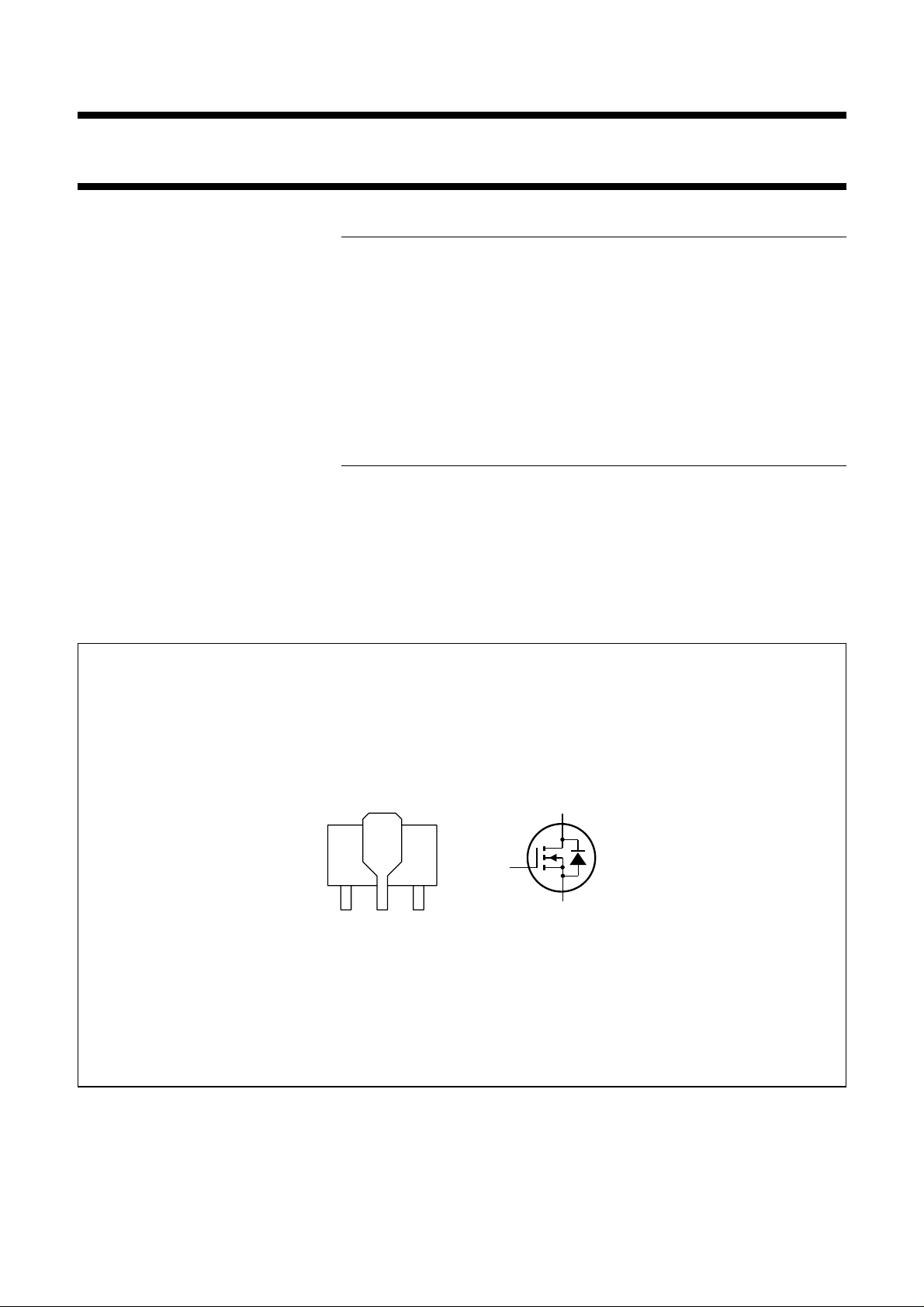
PIN CONFIGURATION
marking: KA
handbook, halfpage
Bottom view
Fig.1 Simplified outline and symbol.
123
d
g
s
MAM355
April 1995 2

Philips Semiconductors Product specification
N-channel enhancement mode vertical
D-MOS transistor
RATINGS
Limiting values in accordance with the Absolute Maximum System (IEC 134)
Drain-source voltage V
Gate-source voltage (open drain) ± V
Drain current (DC) I
Drain current (peak) I
Total power dissipation up to T
amb
=25°C
Storage temperature range T
Junction temperature T
THERMAL RESISTANCE
From junction to ambient
(1)
Note
1. Transistor mounted on ceramic substrate area 2.5 cm
CHARACTERISTICS
=25°C unless otherwise specified
T
j
Drain-source breakdown voltage
I
= 250 µA; VGS=0 V
D
Drain-source leakage current
V
= 60 V; VGS=0
DS
VDS= 200 V; VGS=0
Gate-source leakage current
V
= 20 V; VDS=0 I
GS
Gate threshold voltage
= 1 mA; VDS=V
I
D
GS
(1)
R
2
, thickness 0.7 mm.
I
I
V
P
DSS
DSS
GSS
DS
GSO
D
DM
tot
stg
j
th j-a
(BR) DSS
GS(th)
BSS87
max. 200 V
max. 20 V
max. 280 mA
max. 1.1 A
max. 1 W
−65 to + 150 °C
max. 150 °C
= 125 K/W
min. 200 V
max.
max.
typ.
max. 100 nA
min.
max.
200
60
100
0.8
2.8VV
nA
µA
nA
Drain-source on-resistance
= 400 mA; VGS=10V R
I
D
Transfer admittance
= 400 mA; VDS= 25 V | Yfs|
I
D
Input capacitance f = 1 MHz;
= 25 V; VGS=0 C
V
DS
Output capacitance f = 1 MHz;
= 25 V; VGS=0 C
V
DS
April 1995 3
DS(on)
iss
oss
max.
typ.
typ.
min.
max.
typ.
max.
typ.
6
4.5ΩΩ
350
140mSmS
6045pF
pF
2515pF
pF
 Loading...