

Philips bss83 DATASHEETS

DISCRETE SEMICONDUCTORS
DATA SH EET
BSS83
MOSFET N-channel enhancement
switching transistor
Product specification
File under Discrete Semiconductors, SC07
April 1991
Philips Semiconductors Product specification
MOSFET N-channel enhancement switching transistor BSS83
DESCRIPTION
Symmetrical insulated-gate silicon
MOS field-effect transistor of the
N-channel enhancement mode type.
The transistor is sealed in a SOT143
envelope and features a low ON
resistance and low capacitances. The
transistor is protected against
excessive input voltages by
integrated back-to-back diodes
between gate and substrate.
APPLICATIONS
• analog and/or digital switch
• switch driver
PINNING
1 = substrate (b)
2 = source
3 = drain
4 = gate
Note
1. Drain and source are
interchangeable.
Marking code:
BSS83 = M74
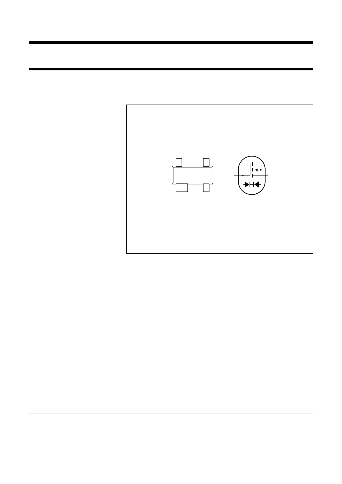
handbook, halfpage
34
g
21
Top view
MAM389
Fig.1 Simplified outline and symbol.
d
b
s
QUICK REFERENCE DATA
Drain-source voltage V
Source-drain voltage V
Drain-substrate voltage V
Source-substrate voltage V
Drain current (DC) I
Total power dissipation up to T
=25°CP
amb
DS
SD
DB
SB
D
tot
max. 10 V
max. 10 V
max. 15 V
max. 15 V
max. 50 mA
max. 230 mW
Gate-source threshold voltage
VDS=VGS;VSB=0;
I
=1µA < 2.0 V
D
V
GS(th)
> 0.1 V
Drain-source ON-resistance
VGS= 10 V; VSB= 0; ID= 0.1 mA R
DSon
< 45 Ω
Feed-back capacitance
VGS=VBS= −15 V;
V
= 10 V; f = 1 MHz C
DS
rss
typ. 0.6 pF
April 1991 2

Philips Semiconductors Product specification
MOSFET N-channel enhancement switching transistor BSS83
RATINGS
Limiting values in accordance with the Absolute Maximum System (IEC 134)
Drain-source voltage V
Source-drain voltage V
Drain-substrate voltage V
Source-substrate voltage V
Drain current (DC) I
Total power dissipation up to T
amb
=25°C
(1)
Storage temperature range T
Junction temperature T
THERMAL RESISTANCE
From junction to ambient in free air
(1)
DS
SD
DB
SB
D
P
tot
stg
j
R
th j-a
max. 10 V
max. 10 V
max. 15 V
max. 15 V
max. 50 mA
max. 230 mW
−65 to + 150 °C
max. 125 °C
= 430 K/W
April 1991 3
 Loading...