

Philips BSS123 Datasheet

DISCRETE SEMICONDUCTORS
DATA SH EET
BSS123
N-channel enhancement mode
vertical D-MOS transistor
Product specification
File under Discrete Semiconductors, SC13b
April 1995

Philips Semiconductors Product specification
N-channel enhancement mode vertical
D-MOS transistor
FEATURES
• Direct interface to C-MOS, TTL,
etc.
• High-speed switching
• No secondary breakdown.
DESCRIPTION
N-channel enhancement mode
vertical D-MOS transistor in a SOT23
envelope, intended for use as a line
current interruptor in telephone sets
and for applications in relay,
high-speed and line transformer
drivers.
PINNING - SOT23
PIN DESCRIPTION
1 gate
2 source
3 drain
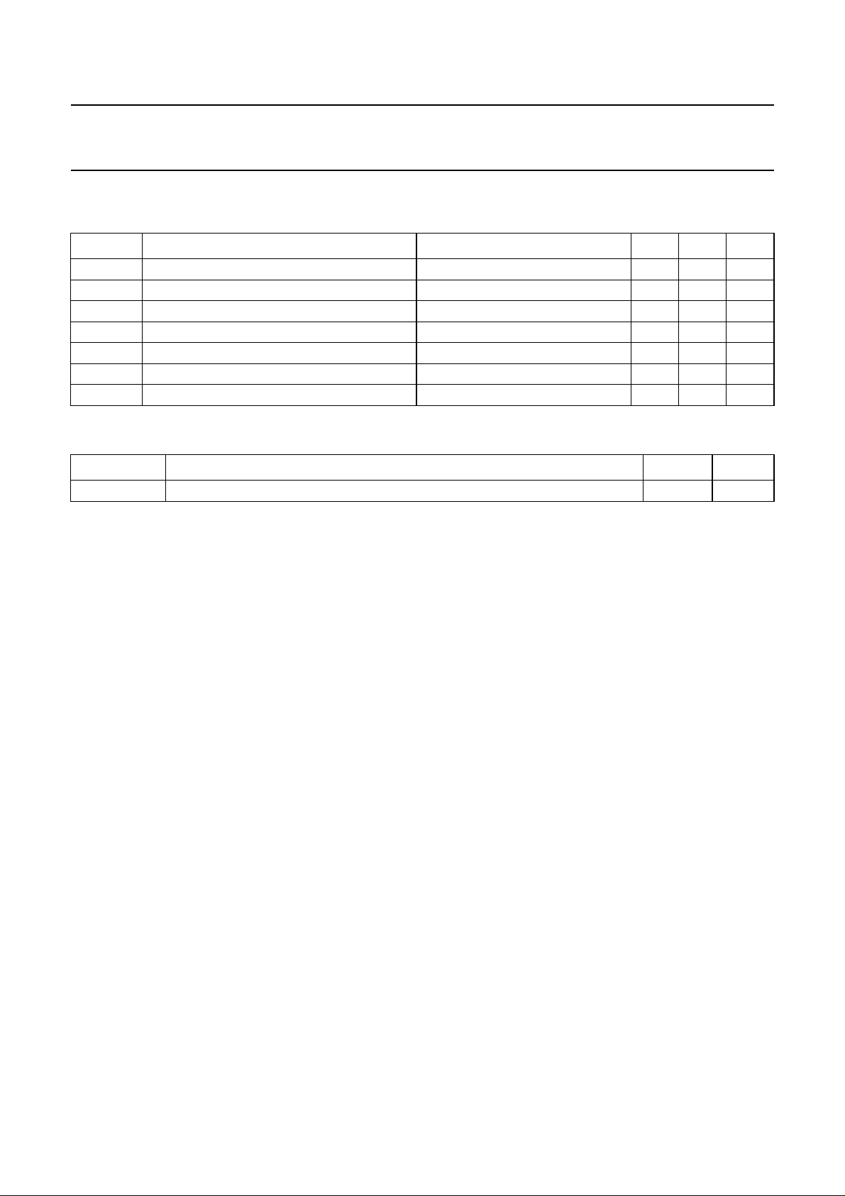
QUICK REFERENCE DATA
SYMBOL PARAMETER CONDITIONS MAX. UNIT
V
DS
I
D
R
DS(on)
V
GS(th)
drain-source voltage 100 V
drain current DC value 150 mA
drain-source on-resistance ID = 120 mA
gate-source threshold voltage ID = 1 mA
PIN CONFIGURATION
dbook, halfpage
VGS = 10 V
VGS = V
3
12
Top view
MSB003
handbook, 2 columns
DS
g
MBB076 - 1
BSS123
6 Ω
2.8 V
d
s
Marking: SA.
Fig.1 Simplified outline and symbol.
April 1995 2
Philips Semiconductors Product specification
N-channel enhancement mode vertical
BSS123
D-MOS transistor
LIMITING VALUES
In accordance with the Absolute Maximum System (IEC 134).
SYMBOL PARAMETER CONDITIONS MIN. MAX. UNIT
V
DS
±V
GSO
I
D
I
DM
P
tot
T
stg
T
j
THERMAL RESISTANCE
SYMBOL PARAMETER VALUE UNIT
R
th j-a
Note
1. Device mounted on a FR4 printboard.
drain-source voltage − 100 V
gate-source voltage open drain − 20 V
drain current DC value − 150 mA
drain current peak value − 600 mA
total power dissipation up to T
= 25 °C − 250 mW
amb
storage temperature range −65 150 °C
junction temperature − 150 °C
from junction to ambient (note 1) 500 K/W
April 1995 3
 Loading...