

Philips BSS110 Datasheet
DISCRETE SEMICONDUCTORS
DATA SH EET
BSS110
P-channel enhancement mode
vertical D-MOS transistor
Product specification
File under Discrete Semiconductors, SC07
Philips Semiconductors
1995 Apr 07
Philips Semiconductors Product specification
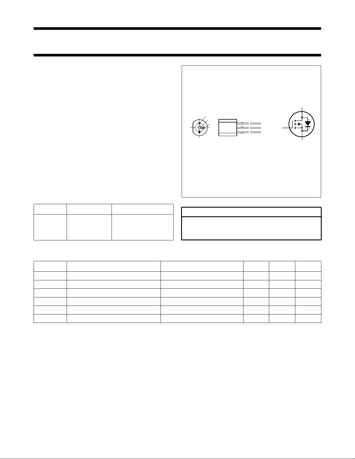
Fig.1 Simplified outline and symbol.
handbook, halfpage
s
d
g
MAM144
1
3
2
QUICK REFERENCE DATA
SYMBOL PARAMETER CONDITIONS MIN. MAX. UNIT
V
DS
drain-source voltage (DC) − −50 V
V
GSO
gate-source voltage (DC) open drain − ±20 V
V
GSth
gate-source threshold voltage ID= −1 mA; VDS= V
GS
−0.8 −2 V
I
D
drain current (DC) − −170 mA
R
DSon
drain-source on-state resistance ID= −170 mA; VGS= −10 V − 10 Ω
P
tot
total power dissipation up to T
amb
= 25 °C − 830 mW
P-channel enhancement mode
vertical D-MOS transistor
FEATURES
• Low threshold voltage
• Direct interface to C-MOS, TTL, etc.
• High speed switching
• No secondary breakdown.
APPLICATIONS
• Intended for use as a Line current interruptor in
telephone sets and for applications in relay, high speed
and line transformer drivers.
DESCRIPTION
P-channel enhancement mode vertical D-MOS transistor
in a TO-92 variant package.
PINNING - TO-92 variant
BSS110
PIN SYMBOL DESCRIPTION
1 s source
2 g gate
3 d drain
The device is supplied in an antistatic package. The
gate-source input must be protected against static
discharge during transport or handling.
CAUTION
1995 Apr 07 2
Philips Semiconductors Product specification
P-channel enhancement mode
BSS110
vertical D-MOS transistor
LIMITING VALUES
In accordance with the Absolute Maximum Rating System (IEC 134).
SYMBOL PARAMETER CONDITIONS MIN. MAX. UNIT
V
DS
V
GSO
I
D
I
DM
P
tot
T
stg
T
j
THERMAL CHARACTERISTICS
SYMBOL PARAMETER CONDITIONS VALUE UNIT
R
th j-a
Note to the “Limiting values” and “Thermal characteristics”
1. Device mounted on a printed-circuit board, maximum lead length 4 mm.
drain-source voltage (DC) − −50 V
gate-source voltage (DC) open drain − ±20 V
drain current (DC) − −170 mA
peak drain current − −520 mA
total power dissipation up to T
= 25 °C; note 1 − 830 mW
amb
storage temperature −65 +150 °C
operating junction temperature − 150 °C
thermal resistance from junction to ambient note 1 150 K/W
CHARACTERISTICS
T
= 25 °C unless otherwise specified.
j
SYMBOL PARAMETER CONDITIONS MIN. TYP. MAX. UNIT
V
(BR)DSS
V
GSth
I
DSS
drain-source breakdown voltage VGS= 0; ID= −10 µA −50 − − V
gate-source threshold voltage VDS= VGS; ID= −1 mA −0.8 − −2 V
drain-source leakage current VGS= 0; VDS= −40 V − − −100 nA
VGS= 0; VDS= −50 V − − −10 µA
VGS= 0; VDS= −50 V; Tj= 125 °C − − −60 µA
I
GSS
R
DSon
gate leakage current VDS= 0; VGS= ±20 V − − ±10 nA
drain-source on-state resistance VGS= −10 V; ID= −170 mA − − 10 Ω
yfs forward transfer admittance VDS= −25 V; ID= −170 mA 50 − − mS
C
iss
C
oss
C
rss
input capacitance VGS= 0; VDS= −25 V; f = 1 MHz − 25 45 pF
output capacitance VGS= 0; VDS= −25 V; f = 1 MHz − 15 25 pF
reverse transfer capacitance VGS= 0; VDS= −25 V; f = 1 MHz − 3.5 12 pF
Switching times (see Figs 2 and 3)
t
on
turn-on time VGS= 0 to −10 V; VDD= −40 V;
− 3 − ns
ID= −200 mA
t
off
turn-off time VGS= −10 to 0 V; VDD= −40 V;
− 7 − ns
ID= −200 mA
1995 Apr 07 3
 Loading...