

Philips BSR43, BSR42, BSR41 Datasheet
DISCRETE SEMICONDUCTORS
DATA SH EET
ook, halfpage
M3D109
BSR40; BSR41; BSR42; BSR43
NPN medium power transistors
Product specification
Supersedes data of 1997 Apr 07
1999 Apr 28
Philips Semiconductors Product specification
NPN medium power transistors BSR40; BSR41; BSR42; BSR43
FEATURES
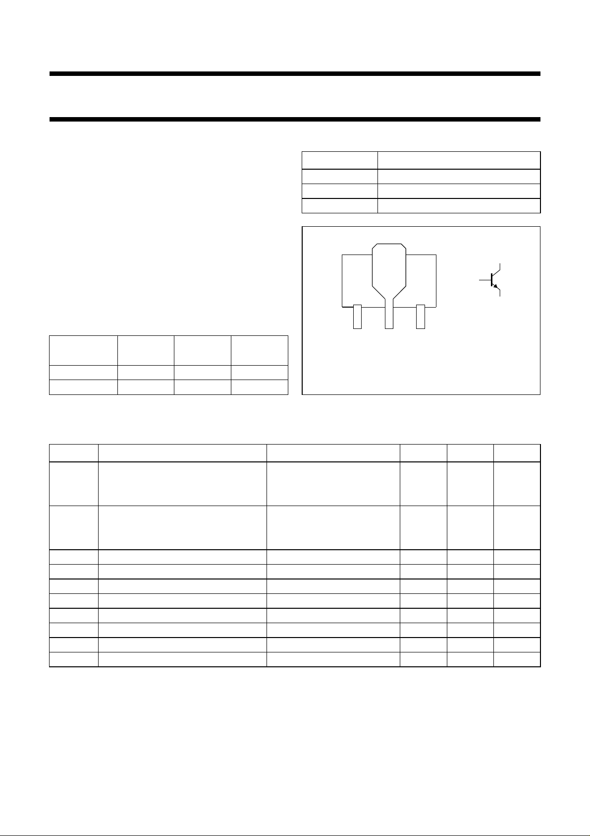
PINNING
• High current (max. 1 A)
• Low voltage (max. 80 V).
APPLICATIONS
• Thick and thin-film circuits
• Telephony and general industrial applications.
handbook, halfpage
DESCRIPTION
NPN medium power transistor in a SOT89 plastic
package. PNP complements: BSR30; BSR3 and BSR33.
MARKING
TYPE
NUMBER
MARKING
CODE
TYPE
NUMBER
MARKING
CODE
BSR40 AR1 BSR42 AR3
BSR41 AR2 BSR43 AR4
LIMITING VALUES
In accordance with the Absolute Maximum Rating System (IEC 134).
PIN DESCRIPTION
1 emitter
2 collector
3 base
2
3
1
123
Bottom view
MAM296
Fig.1 Simplified outline (SOT89) and symbol.
SYMBOL P ARAMETER CONDITIONS MIN. MAX. UNIT
V
CBO
collector-base voltage open emitter
BSR40; BSR41 − 70 V
BSR42; BSR43 − 90 V
V
CEO
collector-emitter voltage open base
BSR40; BSR41 − 60 V
BSR42; BSR43 − 80 V
V
EBO
I
C
I
CM
I
BM
P
tot
T
stg
T
j
T
amb
emitter-base voltage open collector − 5V
collector current (DC) − 1A
peak collector current − 2A
peak base current − 0.2 A
total power dissipation T
≤ 25 °C; note 1 − 1.35 W
amb
storage temperature −65 +150 °C
junction temperature − 150 °C
operating ambient temperature −65 +150 °C
Note
2
1. Device mounted on a printed-circuit board, single sided copper, tinplated, mounting pad for collector 6 cm
For other mounting conditions, see
“Thermal considerations for SOT89 in the General Part of associated Handbook”.
.
1999 Apr 28 2
Philips Semiconductors Product specification
NPN medium power transistors BSR40; BSR41; BSR42; BSR43
THERMAL CHARACTERISTICS
SYMBOL PARAMETER CONDITIONS VALUE UNIT
R
th j-a
R
th j-s
Note
1. Device mounted on a printed-circuit board, single sided copper, tinplated, mounting pad for collector 6 cm2.
For other mounting conditions, see
CHARACTERISTICS
=25°C unless otherwise specified.
T
amb
SYMBOL PARAMETER CONDITIONS MIN. MAX. UNIT
I
CBO
I
EBO
h
FE
V
CEsat
V
BEsat
C
c
C
e
f
T
Switching times (between 10% and 90% levels)
t
on
t
off
thermal resistance from junction to ambient note 1 93 K/W
thermal resistance from junction to soldering point 13 K/W
“Thermal considerations for SOT89 in the General Part of associated Handbook”.
collector cut-off current IE= 0; VCB=60V − 100 nA
I
= 0; VCB=60V; Tj= 150 °C − 50 µA
E
emitter cut-off current IC= 0; VEB=5V − 100 nA
DC current gain IC= 100 µA; VCE= 5 V; note 1
BSR40; BSR42 10 −
BSR41; BSR43 30 −
DC current gain I
= 100 mA; VCE= 5 V; note 1
C
BSR40; BSR42 40 120
BSR41; BSR43 100 300
DC current gain I
= 500 mA; VCE= 5 V; note 1
C
BSR40; BSR42 30 −
BSR41; BSR43 50 −
collector-emitter saturation voltage IC= 150 mA; IB= 15 mA; note 1 − 250 mV
I
= 500 mA; IB= 50 mA; note 1 − 500 mV
C
base-emitter saturation voltage IC= 150 mA; IB= 15 mA; note 1 − 1V
= 500 mA; IB= 50 mA; note 1 − 1.2 V
I
C
collector capacitance IE=ie= 0; VCB= 10 V; f = 1 MHz − 12 pF
emitter capacitance IC=ic= 0; VEB= 0.5 V; f = 1 MHz − 90 pF
transition frequency IC= 50 mA; VCE= 10 V; f = 100 MHz 100 − MHz
turn-on time I
turn-off time − 1 µs
= 100 mA; I
Con
I
= −5mA
Boff
Bon
= 5 mA;
− 250 ns
Note
1. Pulse test: t
≤ 300 µs; δ≤0.01.
p
1999 Apr 28 3
 Loading...