

Philips bsr12 DATASHEETS

DISCRETE SEMICONDUCTORS
DATA SH EET
ook, halfpage
M3D088
BSR12
PNP switching transistor
Product specification 1999 Jul 23
Philips Semiconductors Product specification
PNP switching transistor BSR12
FEATURES
• Low current (max. 100 mA)
• Low voltage (max. 15 V).
APPLICATIONS
• High-speed, saturated switching applications for
industrial service in thick and thin-film circuits.
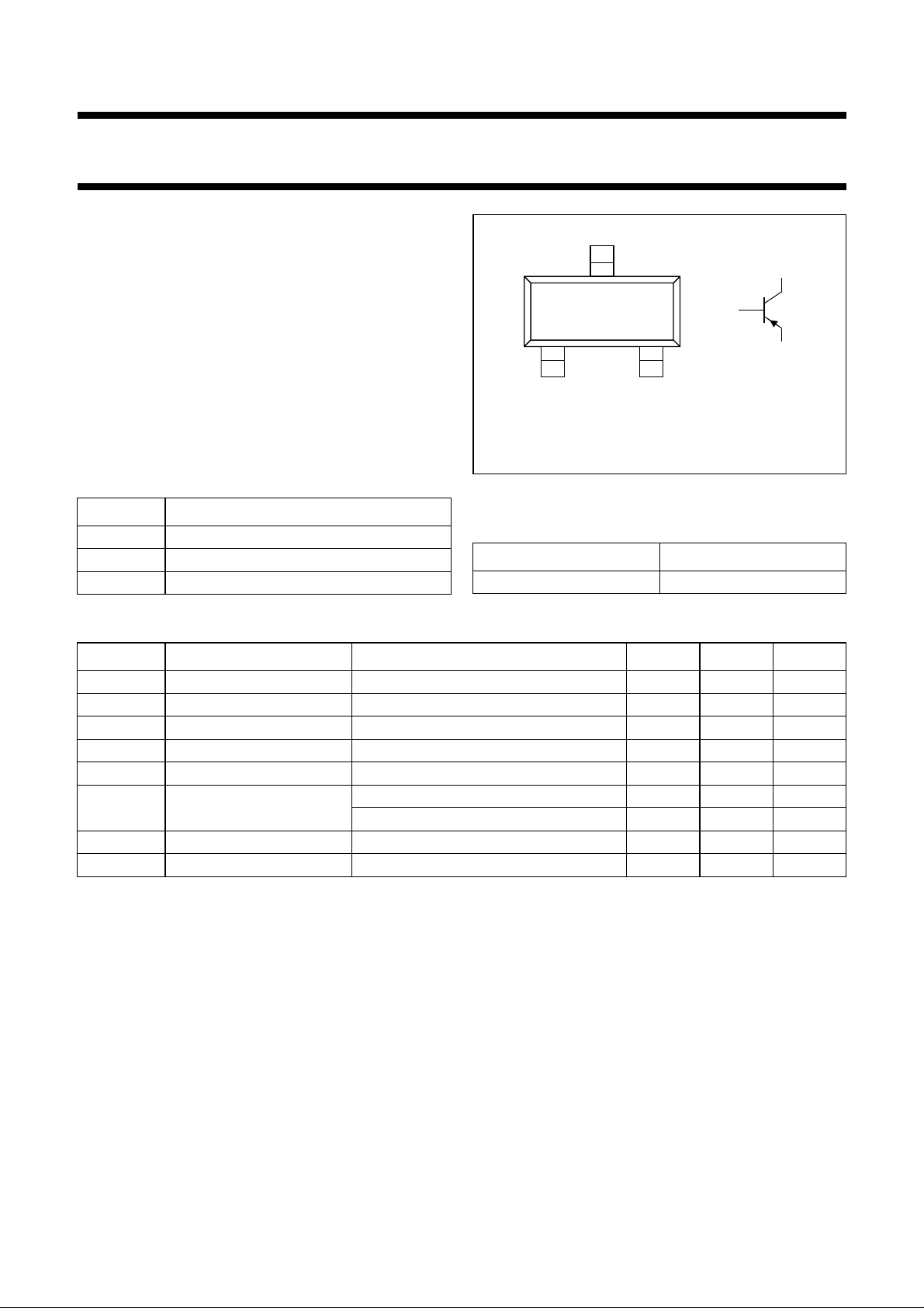
handbook, halfpage
Top view
3
1
21
MAM256
3
2
DESCRIPTION
PNP switching transistor in a SOT23 plastic package.
Fig.1 Simplified outline (SOT23) and symbol.
PINNING
PIN DESCRIPTION
1 base
2 emitter
3 collector
MARKING
TYPE NUMBER MARKING CODE
BSR12 B5p
QUICK REFERENCE DATA
SYMBOL PARAMETER CONDITIONS MIN. MAX. UNIT
V
V
I
P
T
h
f
t
CBO
CEO
CM
tot
j
FE
T
off
collector-base voltage open emitter −−15 V
collector-emitter voltage open base −−15 V
peak collector current −−200 mA
total power dissipation T
≤ 25 °C − 250 mW
amb
junction temperature − 150 °C
DC current gain IC= −10 mA; VCE= −1V 30 −
=−50 mA; VCE= −1 V 30 120
I
C
transition frequency f = 500 MHz; IC= −50 mA; VCE= −10 V 1.5 − GHz
turn-off time I
= −30 mA; I
Con
= −3 mA; I
Bon
= 3mA − 30 ns
Boff
1999 Jul 23 2
Philips Semiconductors Product specification
PNP switching transistor BSR12
LIMITING VALUES
In accordance with the Absolute Maximum Rating System (IEC 134).
SYMBOL PARAMETER CONDITIONS MIN. MAX. UNIT
V
CBO
V
CEO
V
EBO
I
C
I
CM
P
tot
T
stg
T
j
THERMAL CHARACTERISTICS
SYMBOL PARAMETER CONDITIONS VALUE UNIT
R
th j-a
collector-base voltage open emitter −−15 V
collector-emitter voltage open base −−15 V
emitter-base voltage open collector −−3V
collector current (DC) −−100 mA
peak collector current −−200 mA
total power dissipation T
≤ 25 °C − 250 mW
amb
storage temperature −65 +150 °C
junction temperature − 150 °C
thermal resistance from junction to
note 1 500 K/W
ambient
Note
1. Transistor mounted on a ceramic substrate 8 × 10 × 0.7 mm.
1999 Jul 23 3
Philips Semiconductors Product specification
PNP switching transistor BSR12
CHARACTERISTICS
T
=25°C unless otherwise specified.
amb
SYMBOL PARAMETER CONDITIONS MIN. TYP. MAX. UNIT
I
CBO
I
CES
V
(BR)CBO
V
(BR)CES
V
(BR)EBO
V
CEOsust
V
CEsat
V
BEsat
h
FE
f
T
C
c
C
e
Switching time (see Fig.2)
t
on
t
off
collector cut-off current IE= 0; VCB= −10 V −−−50 nA
I
=0;VCB= −10 V; T
E
= 125 °C −−−5µA
amb
collector cut-off current VBE= 0; VCE= −10 V −−−50 nA
breakdown voltage IE= 0; IC= −10 µA −15 −−V
breakdown voltage VBE= 0; IC= −10 µA −15 −−V
breakdown voltage IC= 0; IE= −100 µA −3 −−V
collector-emittersustaining
IB= 0; IC= −10 mA −15 −−V
voltage
collector-emitter saturation
voltage
base-emitter saturation
voltage
IC= −10 mA; IB= −1 mA; note 1 −−−130 mV
I
= −50 mA; IB= −5 mA; note 1 −−180 −270 mV
C
= −100 mA; IB= −10 mA; note 1 −−−450 mV
I
C
IC= −10 mA; IB= −1 mA; note 1 −725 −−920 mV
I
= −50 mA; IB= −5 mA; note 1 −800 −−1150 mV
C
I
= −100 mA; IB= −10 mA; note 1 −900 −−1500 mV
C
DC current gain IC= −1 mA; VCE= −1 V; note 1 30 −−
I
=−10 mA; VCE= −1 V; note 1 30 −−
C
I
=−50 mA; VCE= −1 V; note 1 30 − 120
C
I
= −50 mA; VCE= −1V;
C
T
=55°C; note 1
amb
I
=−100 mA; VCE= −1 V; note 1 20 −−
C
transition frequency IC = −50 mA; VCE= −10 V;
30 −−
1.5 −−GHz
f = 500 MHz
collector capacitance IE=Ie= 0; VCB= −5V −−4.5 pF
emitter capacitance IC=Ic= 0; VEB= −0.5 V −−6pF
turn-on time Vi=−6.85 V; VBB=0V;
I
= −30 mA; I
Con
= −3.0 mA
Bon
turn-off time Vi= 11.7 V; VBB=−9.85 V;
I
= −30 mA; I
Con
I
=3mA
Boff
Bon
= −3 mA;
−−20 ns
−−30 ns
Note
1. Pulse test: t
= 300 µs; δ = 0.01.
p
1999 Jul 23 4
 Loading...