

Philips BSP255 Datasheet

DISCRETE SEMICONDUCTORS
DATA SH EET
BSP255
P-channel enhancement mode
vertical D-MOS transistor
Product specification
Supersedes data of 1996 Jun 13
File under Discrete Semiconductors, SC07
1996 Aug 05
Philips Semiconductors Product specification
P-channel enhancement mode
vertical D-MOS transistor
FEATURES
• Direct interface to C-MOS, TTL etc
• Low threshold voltage
• High speed switching
• No secondary breakdown.
APPLICATIONS
• Line current interrupter in telephone sets
• Relay, high speed and line transformer drivers.
DESCRIPTION
P-channel enhancement mode vertical D-MOS transistor
in a 4-pin plastic SOT223 SMD package.
CAUTION
The device is supplied in an antistatic package. The
gate-source input must be protected against static
discharge during transport or handling.
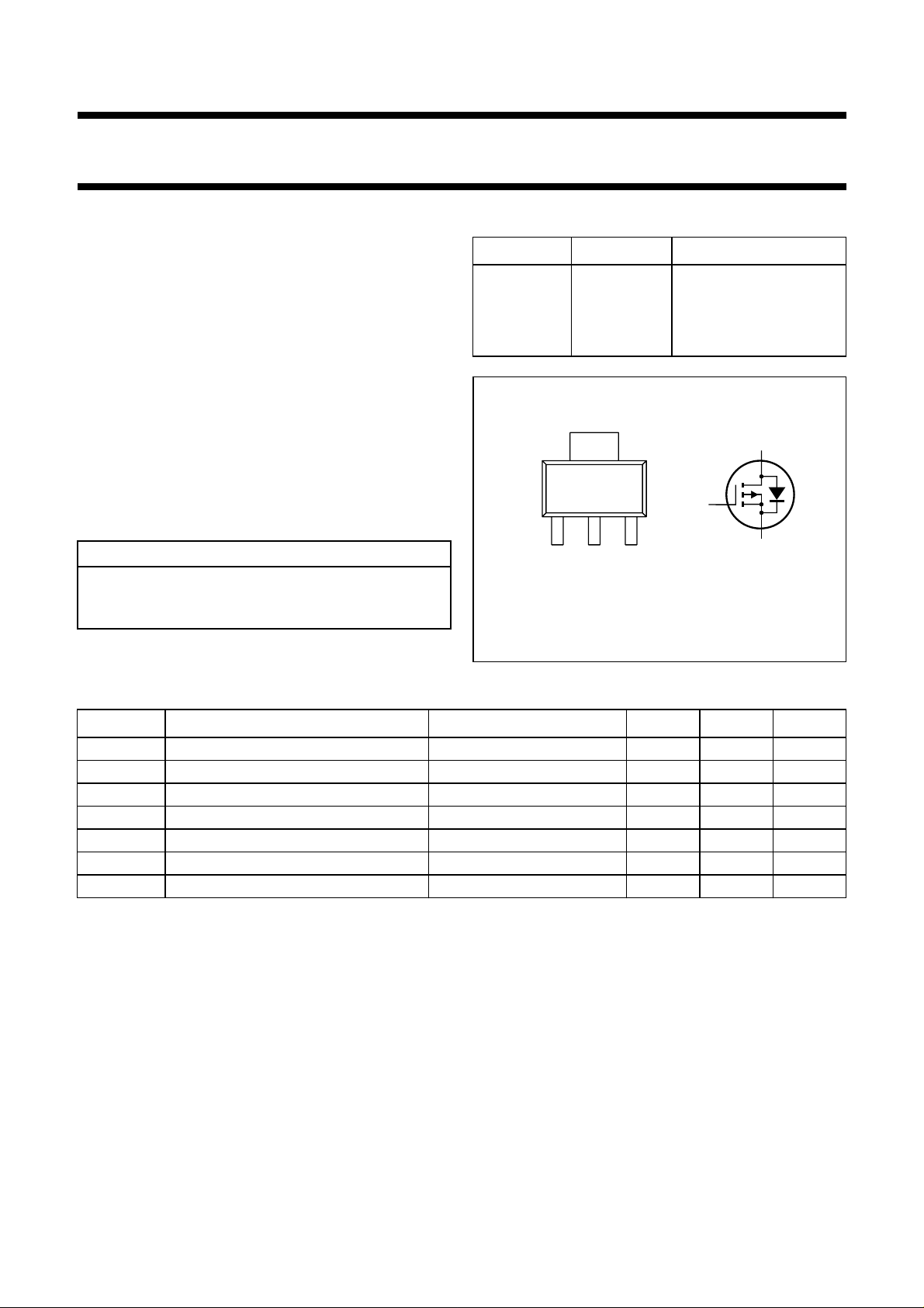
PINNING - SOT223
PIN SYMBOL DESCRIPTION
1 g gate
2 d drain
3 s source
4 d drain
handbook, halfpage
123
Top view
4
g
MAM121
Fig.1 Simplified outline and symbol.
BSP255
d
s
QUICK REFERENCE DATA
SYMBOL PARAMETER CONDITIONS MIN. MAX. UNIT
V
DS
V
SD
V
GS
V
GSth
I
D
R
DSon
P
tot
drain-source voltage (DC) −−300 V
source-drain diode forward voltage IS= −0.5 A −−1.8 V
gate-source voltage (DC) −±20 V
gate-source threshold voltage ID= −1 mA; VDS=V
GS
−0.8 −2V
drain current (DC) Ts= 100 °C −−325 mA
drain-source on-state resistance ID= −160 mA; VGS= −10 V − 17 Ω
total power dissipation Ts= 100 °C − 4W
1996 Aug 05 2

Philips Semiconductors Product specification
P-channel enhancement mode
BSP255
vertical D-MOS transistor
LIMITING VALUES
In accordance with the Absolute Maximum Rating System (IEC 134).
SYMBOL PARAMETER CONDITIONS MIN. MAX. UNIT
V
DS
V
GS
I
D
I
DM
P
tot
T
stg
T
j
Source-drain diode
I
S
I
SM
Notes
1. T
s
2. Pulse width and duty cycle limited by maximum junction temperature.
drain-source voltage (DC) −−300 V
gate-source voltage (DC) −±20 V
drain current (DC) Ts= 100 °C; note 1 −−325 mA
peak drain current note 2 −−1.3 A
total power dissipation Ts= 100 °C − 4W
storage temperature −65 +150 °C
operating junction temperature −65 +150 °C
source current (DC) Ts= 100 °C −−0.5 A
peak pulsed source current note 2 −−2A
is the temperature at the soldering point of the drain lead.
10
handbook, halfpage
P
tot
(W)
8
6
4
2
0
0 200
50 100 150
Ts (oC)
Fig.2 Power derating curve.
MBH446
−10
handbook, halfpage
I
D
(A)
−1
−1
−10
P
−2
−10
−3
−10
−1
δ =0.01; TS= 100 °C.
(1) R
DSon limitation
(1)
t
=
δ
T
t
p
T
−10
.
Fig.3 DC SOAR.
MBH445
tp =
10 µs
100 µs
1 ms
2
10 ms
VDS (V)
−10
3
p
DC
t
−10
1996 Aug 05 3
 Loading...