

Philips BSP225 Datasheet

DISCRETE SEMICONDUCTORS
DATA SH EET
BSP225
P-channel enhancement mode
vertical D-MOS transistor
Product specification
File under Discrete Semiconductors, SC13b
April 1995
Philips Semiconductors Product specification
P-channel enhancement mode vertical
D-MOS transistor
FEATURES
• Low R
DS(on)
• Direct interface to C-MOS, TTL,
etc.
• High-speed switching
• No secondary breakdown.
DESCRIPTION
P-channel enhancement mode
vertical D-MOS transistor in a
miniature SOT223 envelope,
intended for use in relay, high-speed
and line transformer drivers.
PINNING - SOT223
PIN DESCRIPTION
1 gate
2 drain
3 source
4 drain
QUICK REFERENCE DATA
SYMBOL PARAMETER CONDITIONS MAX. UNIT
−V
−I
R
DS(on)
−V
DS
D
GS(th)
drain-source voltage 250 V
drain current DC value 225 mA
drain-source on-resistance −ID = 200 mA
gate-source threshold voltage −ID = 1 mA
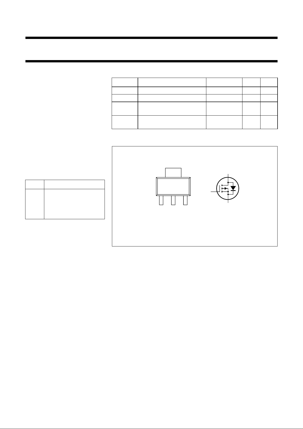
PIN CONFIGURATION
handbook, halfpage
123
Top view
BSP225
15 Ω
−VGS = 10 V
2.8 V
VGS = V
4
g
MAM121
DS
d
s
Fig.1 Simplified outline and symbol.
April 1995 2
Philips Semiconductors Product specification
P-channel enhancement mode vertical
BSP225
D-MOS transistor
LIMITING VALUES
In accordance with the Absolute Maximum System (IEC 134).
SYMBOL P ARAMETER CONDITIONS MIN. MAX. UNIT
−V
DS
±V
GSO
−I
D
−I
DM
P
tot
T
stg
T
j
Note
1. Device mounted on an epoxy printed-circuit board, 40 x 40 x 1.5 mm, mounting pad for the drain lead minimum 6 cm
THERMAL RESISTANCE
SYMBOL PARAMETER VALUE UNIT
R
th j-a
drain-source voltage − 250 V
gate-source voltage open drain − 20 V
drain current DC value − 225 mA
drain current peak value − 600 mA
total power dissipation up to T
= 25 °C (note 1) − 1.5 W
amb
storage temperature range −65 150 °C
junction temperature − 150 °C
from junction to ambient (note 1) 83.3 K/W
2
.
Note
1. Device mounted on an epoxy printed-circuit board, 40 x 40 x 1.5 mm, mounting pad for the drain lead minimum 6 cm
2
.
April 1995 3

Philips Semiconductors Product specification
P-channel enhancement mode vertical
BSP225
D-MOS transistor
CHARACTERISTICS
T
= 25 °C unless otherwise specified.
j
SYMBOL PARAMETER CONDITIONS MIN. TYP. MAX. UNIT
−V
(BR)DSS
drain-source breakdown voltage −ID = 10 µA
VGS = 0
−I
DSS
drain-source leakage current −VDS = 200 V
VGS = 0
±I
GSS
gate-source leakage current VDS = 0
±VGS = 20 V
−V
GS(th)
gate-source threshold voltage −ID = 1 mA
VGS = V
R
DS(on)
drain-source on-resistance −ID = 200 mA
−VGS = 10 V
Y
transfer admittance −ID = 200 mA
fs
−VDS = 25 V
C
iss
input capacitance −VDS = 25 V
−VGS = 0
f = 1 MHz
C
oss
output capacitance −VDS = 25 V
−VGS = 0
f = 1 MHz
C
rss
feedback capacitance −VDS = 25 V
−VGS = 0
f = 1 MHz
DS
250 −− V
−−1 µA
−−100 nA
0.8 − 2.8 V
− 10 15 Ω
100 200 − mS
− 65 90 pF
− 20 30 pF
− 615pF
Switching times (see Figs 2 and 3)
t
on
t
off
turn-on time −ID = 250 mA
turn-off time −ID = 250 mA
−VDD = 50 V
−VGS = 0 to 10 V
−VDD = 50 V
= 0 to 10 V
−V
GS
− 510ns
− 20 30 ns
April 1995 4
 Loading...