

Philips BSP090 Datasheet
DISCRETE SEMICONDUCTORS
DATA SH EET
BSP090
P-channel enhancement mode
vertical D-MOS transistor
Product specification
Supersedes data of 1997 Jan 20
File under Discrete Semiconductors, SC07
1997 Mar 13
Philips Semiconductors Product specification
P-channel enhancement mode vertical
D-MOS transistor
FEATURES
• High speed switching
• No secondary breakdown
• Very low on-state resistance.
APPLICATIONS
• Motor and actuator drivers
• Power management
• Synchronized rectification.
DESCRIPTION
P-channel enhancement mode vertical D-MOS transistor
in a 4-pin plastic SOT223 SMD package.
CAUTION
The device is supplied in an antistatic package.
The gate-source input must be protected against static
discharge during transport or handling.
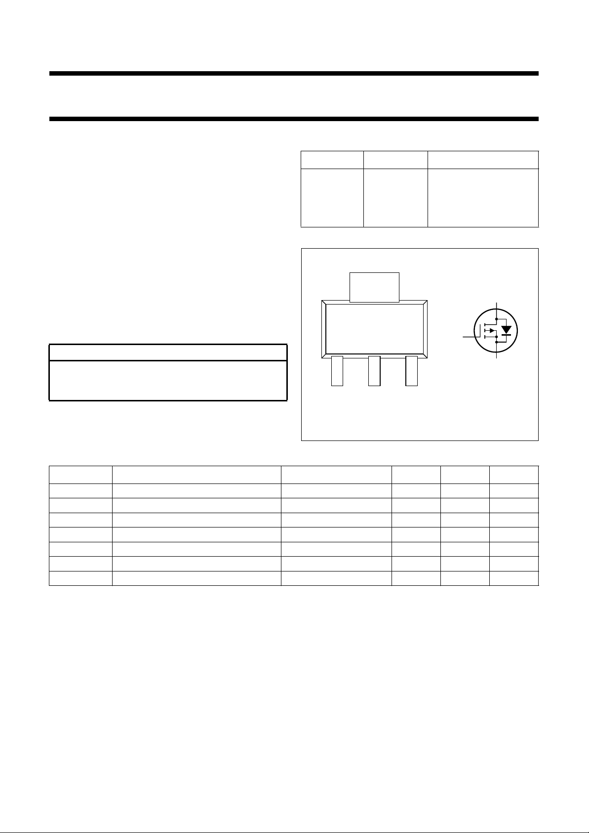
PINNING - SOT223
PIN SYMBOL DESCRIPTION
1 g gate
2 d drain
3 s source
4 d drain
handbook, halfpage
123
Top view
4
g
MAM121
BSP090
d
s
Fig.1 Simplified outline and symbol.
QUICK REFERENCE DATA
SYMBOL PARAMETER CONDITIONS MIN. MAX. UNIT
V
V
V
V
I
D
R
P
DS
SD
GS
GSth
DSon
tot
drain-source voltage (DC) −−30 V
source-drain diode forward voltage IS= −1.25 A −−1.3 V
gate-source voltage (DC) −±20 V
gate-source threshold voltage ID= −1 mA; VDS=V
−1 −2.8 V
GS
drain current (DC) Ts= 100 °C −−5.7 A
drain-source on-state resistance ID= −2.8 A; VGS= −10 V − 0.09 Ω
total power dissipation Ts= 100 °C − 5W
1997 Mar 13 2
Philips Semiconductors Product specification
P-channel enhancement mode vertical
BSP090
D-MOS transistor
LIMITING VALUES
In accordance with the Absolute Maximum Rating System (IEC 134).
SYMBOL PARAMETER CONDITIONS MIN. MAX. UNIT
V
DS
V
GS
I
D
I
DM
P
tot
T
stg
T
j
Source-drain diode
I
S
I
SM
Notes
1. T
s
2. Pulse width and duty cycle limited by maximum junction temperature.
3. Device mounted on a printed-circuit board with a R
4. Device mounted on a printed-circuit board with a R
drain-source voltage (DC) −−30 V
gate-source voltage (DC) −±20 V
drain current (DC) Ts= 100 °C; note 1 −−5.7 A
peak drain current note 2 −−22 A
total power dissipation Ts= 100 °C − 5W
=25°C; note 3 − 3.3 W
T
amb
=25°C; note 4 − 1.25 W
T
amb
storage temperature −65 +150 °C
operating junction temperature −65 +150 °C
source current (DC) Ts= 100 °C −−3.8 A
peak pulsed source current note 2 −−15 A
is the temperature at the soldering point of the drain lead.
(ambient to tie-point) of 27.5 K/W.
th a-tp
(ambient to tie-point) of 90 K/W.
th a-tp
THERMAL CHARACTERISTICS
SYMBOL PARAMETER VALUE UNIT
R
th j-s
thermal resistance from junction to soldering point 10 K/W
1997 Mar 13 3
Philips Semiconductors Product specification
P-channel enhancement mode vertical
D-MOS transistor
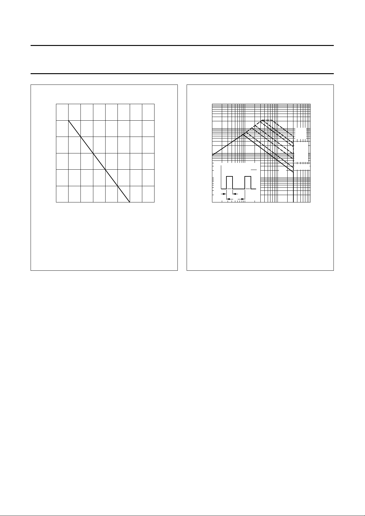
150
MGD716
Ts (°C)
15
handbook, halfpage
P
tot
(W)
10
5
0
0
50 100 200
2
−10
handbook, halfpage
I
D
(A)
−10
−1
−1
−10
−2
−10
−1
−10
BSP090
MGD727
(1)
t
P
t
p
T
p
δ =
T
t
−1
−10 −10
DC
10 µs
50 µs
100 µs
1 ms
10 ms
100 ms
VDS (V)
t
p =
2
Fig.2 Power derating curve.
δ = 0.01; Ts= 100 °C.
(1) R
DSon
limitation.
Fig.3 SOAR.
1997 Mar 13 4
 Loading...