

Philips BSN254A, BSN254 Datasheet

DISCRETE SEMICONDUCTORS
DATA SH EET
BSN254
BSN254A
N-channel enhancement mode
vertical D-MOS transistors
Product specification
File under Discrete Semiconductors, SC13b
April 1995

Philips Semiconductors Product specification
N-channel enhancement mode vertical
D-MOS transistors
DESCRIPTION
N-channel enhancement mode
vertical D-MOS transistors in TO-92
variant envelope and designed for
use as line current interrupters in
telephone sets and for application in
relay, high-speed and
line-transformer drivers.
FEATURES
• Direct interface to C-MOS, TTL,
etc.
• High-speed switching
• No second breakdown
• Low R
DS (on)
QUICK REFERENCE DATA
Drain-source voltage V
Drain current (DC) I
Total power dissipation up to T
Drain-source on-resistance
ID= 300 mA; VGS=10V R
Gate-source threshold voltage V
PINNING (BSN254)
1 = gate
2 = drain
3 = source
PINNING (BSN254A)
1 = source
2 = gate
3 = drain
=25°CP
amb
DS
D
tot
DS(on)
GS(th)
BSN254
BSN254A
max. 250 V
max. 300 mA
max. 1 W
typ.
max.
max. 2 V
5.0
7.0ΩΩ
PIN CONFIGURATION - TO-92 VARIANT
handbook, halfpage
1
Note: Various pinnings are available on request.
2
3
g
MAM146
Fig.1 Simplified outline and symbol.
d
s
April 1995 2

Philips Semiconductors Product specification
N-channel enhancement mode vertical
D-MOS transistors
BSN254
BSN254A
RATINGS
Limiting values in accordance with the Absolute Maximum System (IEC 134)
Drain-source voltage V
Gate-source voltage (open drain) ± V
Drain current (DC) I
Drain current (peak) I
Total power dissipation up to T
=25°C (note 1) P
amb
D
DM
Storage temperature range T
Junction temperature T
DS
GSO
tot
stg
j
max. 250 V
max. 20 V
max. 300 mA
max. 1.2 A
max. 1 W
−65 to + 150 °C
max. 150 °C
THERMAL RESISTANCE
From junction to ambient (note 1) R
th j-a
= 125 K/W
Note
1. Device mounted on printed-circuit board, max. lead length 4 mm, mounting pad for drain lead min. 10 mm × 10 mm.
CHARACTERISTICS
=25°C unless otherwise specified
T
j
Drain-source breakdown voltage
=10µA; VGS=0 V
D
(BR) DSS
min. 250 VI
Drain-source leakage current
= 200 V; VGS=0 I
DS
Gate-source leakage current
=20V; VDS=0 ±I
GS
Gate threshold voltage
I
= 1 mA; VDS=V
D
GS
Drain-source on-resistance
= 300 mA; VGS=10V R
I
D
ID= 20 mA; VGS= 2.4 V R
Transfer admittance
ID= 300 mA; VDS=25V Yfs
Input capacitance at f = 1 MHz
= 25 V; VGS=0 C
V
DS
DSS
V
GS(th)
DS (on)
DS(on)
iss
GSS
max. 1 µAV
max. 100 nA± V
min.
max.
typ.
max.
0.8
2.0VV
5.0
7.0ΩΩ
max. 10 Ω
min.
typ.
typ.
200
400mSmS
6590pF
max.
pF
April 1995 3
Philips Semiconductors Product specification
N-channel enhancement mode vertical
D-MOS transistors
Output capacitance at f=1MHz
= 25 V; VGS=0 C
DS
Feedback capacitance at f=1MHz
= 25 V; VGS=0 C
V
DS
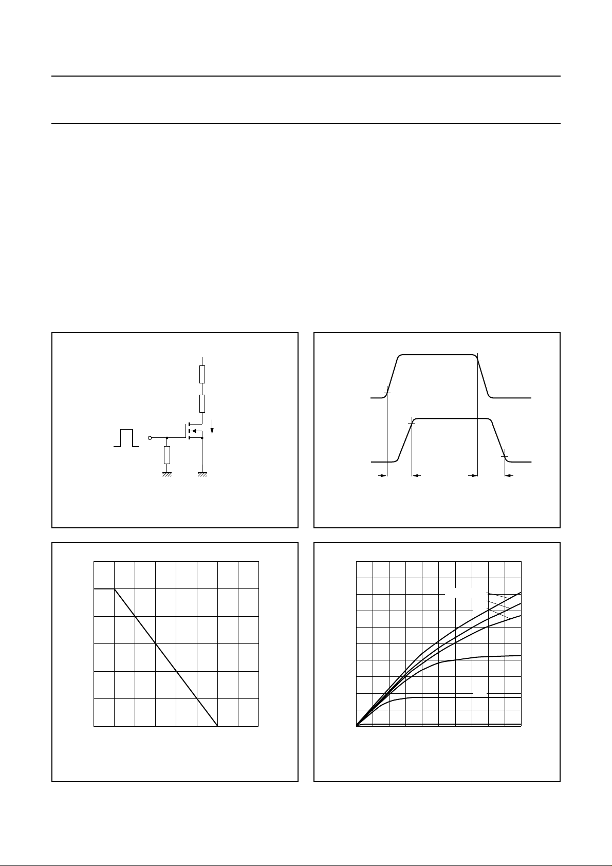
Switching times (see Figs 2 and 3)
I
= 250 mA; VDD=50V; VGS= 0 to 10 V t
D
handbook, halfpage
VDD = 50 V
oss
rss
on
t
off
handbook, halfpage
INPUT
typ.
max.
typ.
max.
typ.
max.
typ.
max.
BSN254
BSN254A
2030pF
pFV
515pF
pF
510ns
ns
2030ns
ns
90 %
10 V
1.2
handbook, halfpage
P
tot
(W)
0.8
0.4
I
0 V
50 Ω
D
MSA631
Fig.2 Switching times test circuit.
MRC238
OUTPUT
Fig.3 Input and output waveforms.
handbook, halfpage
2
I
D
(A)
1.6
1.2
0.8
10 %
t
on
90 %
VGS = 10 V
6 V
5 V
4 V
t
off
10 %
MBB692
MDA712
0
0
50 100 200150
T
amb
(°C)
Fig.4 Power derating curve.
April 1995 4
0.4
0
010
246
3 V
2 V
8
VDS (V)
Fig.5 Output characteristics; Tj=25°C; typical
values.
 Loading...