

Philips bsn20w DATASHEETS
DISCRETE SEMICONDUCTORS
DATA SH EET
ook, halfpage
M3D102
BSN20W
N-channel enhancement mode
vertical D-MOS transistor
Product specification
Supersedes data of 1997 Jun 20
2000 Mar 10
Philips Semiconductors Product specification
N-channel enhancement mode
vertical D-MOS transistor
FEATURES
• Direct interface to C-MOS, TTL, etc.
• High-speed switching
• No secondary breakdown.
APPLICATIONS
• Thin and thick film circuits
• General purpose fast switching applications.
DESCRIPTION
N-channel enhancement mode vertical D-MOS transistor
in a 3 pin plastic SOT323 SMD package.
CAUTION
The device is supplied in an antistatic package. The
gate-source input must be protected against static
discharge during transport or handling.
BSN20W
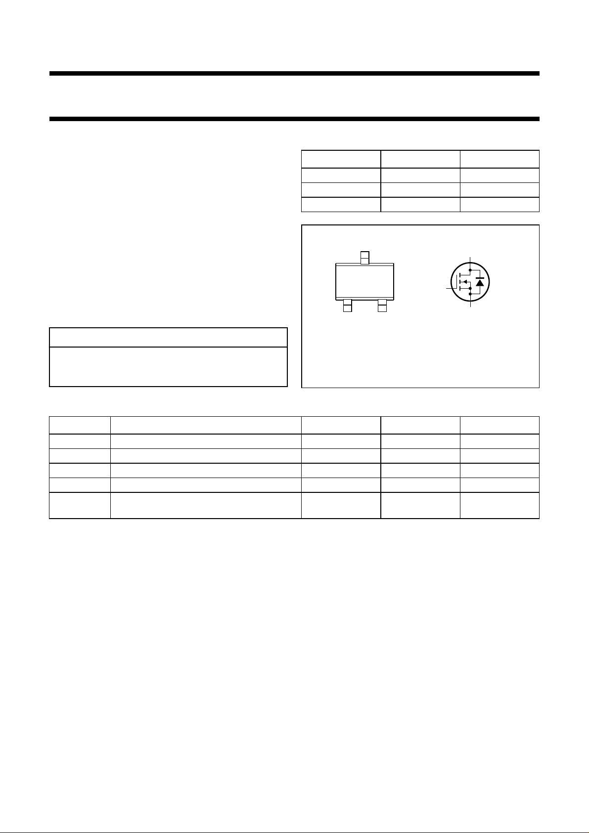
PINNING - SOT323
PIN SYMBOL DESCRIPTION
1 g gate
2 s source
3 d drain
handbook, halfpage
12
Top view
Marking code: M8- =made in Hong Kong; M8t = made in Malaysia
(or Bangkok).
3
MAM356
Fig.1 Simplified outline and symbol.
d
g
s
QUICK REFERENCE DATA
SYMBOL PARAMETER CONDITIONS MAX. UNIT
V
V
I
D
R
P
DS
GSth
DSon
tot
drain-source voltage (DC) 50 V
gate-source threshold voltage 1.8 V
drain current (DC) 80 mA
drain-source on-state resistance 15 Ω
total power dissipation T
amb
≤ 25 °C;
200 mW
note 1
Note
1. Device mounted on a printed-circuit board.
2000 Mar 10 2
Philips Semiconductors Product specification
N-channel enhancement mode
BSN20W
vertical D-MOS transistor
LIMITING VALUES
In accordance with the Absolute Maximum Rating System (IEC 60134).
SYMBOL PARAMETER CONDITIONS MIN. MAX. UNIT
V
DS
V
GSO
I
D
I
DM
P
tot
T
stg
T
j
Note
1. Device mounted on a printed-circuit board.
THERMAL CHARACTERISTICS
SYMBOL PARAMETER CONDITIONS VALUE UNIT
R
th j-a
drain-source voltage (DC) − 50 V
gate-source voltage (DC) open drain −±20 V
drain current (DC) − 80 mA
peak drain current − 300 mA
total power dissipation T
≤ 25 °C; note 1 − 200 mW
amb
storage temperature −65 +150 °C
operating junction temperature −65 +150 °C
thermal resistance from junction to ambient note 1 625 K/W
CHARACTERISTICS
=25°C unless otherwise specified.
T
j
SYMBOL PARAMETER CONDITIONS MIN. TYP. MAX. UNIT
V
(BR)DSS
V
GSth
I
DSS
I
GSS
R
DSon
C
iss
C
oss
C
rss
drain-source breakdown voltage VGS= 0; ID=10µA50−−V
gate-source threshold voltage VGS=VDS; ID= 1 mA 0.4 − 1.8 V
drain-source leakage current VGS= 0; VDS=40V −−1µA
gate-source leakage current VGS= ±20 V; VDS=0 −−±100 nA
drain-source on-state resistance VGS= 10 V; ID=80mA − 815Ω
V
=5V; ID=80mA − 14 20 Ω
GS
= 2.5 V; ID=10mA − 18 30 Ω
V
GS
input capacitance VGS= 0; VDS=10V; f=1MHz − 815pF
output capacitance VGS= 0; VDS=10V; f=1MHz − 715pF
reverse transfer capacitance VGS= 0; VDS=10V; f=1MHz − 25pF
Switching times
t
on
turn-on time VGS= 0 to 10 V; VDD=20V;
− 25ns
ID=80mA
t
off
turn-off time VGS=10to0V; VDD=20V;
− 510ns
ID=80mA
2000 Mar 10 3
 Loading...