Philips BSH301 Datasheet

DISCRETE SEMICONDUCTORS
DATA SH EET
BSH301
Dual N-channel enhancement
mode MOS transistor
Objective specification
1999 Apr 06

Philips Semiconductors Objective specification
Dual N-channel enhancement mode MOS transistor BSH301
FEATURES
• 40 mΩ on-state resistance at 2.5 V gate drive
• R
rating down to 1.8 V
DSon
• ESD gate protection.
APPLICATIONS
• Li-Ion safety switch
• Power management.
handbook, halfpage
8
5
d1s2s
2
g
2
d1s1s
DESCRIPTION
Two N-channel enhancement mode MOS transistors in an
1
4
MAM423
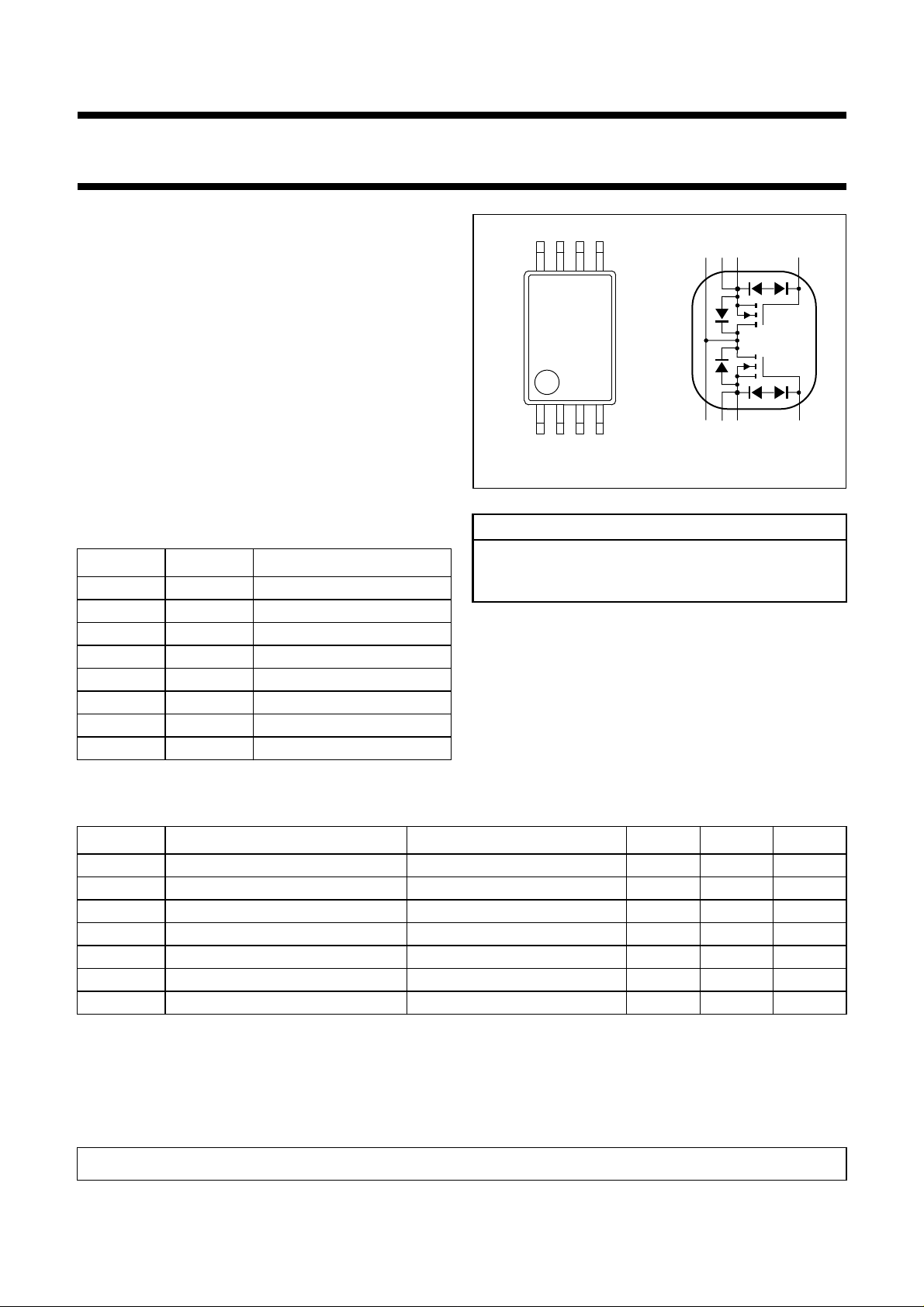
Fig.1 Simplified outline (SOT530) and symbol.
1
8-pin plastic TSSOP8 package.
PINNING SOT530 (TSSOP8)
PIN SYMBOL DESCRIPTION
1 d1 drain 1
The device is supplied in an antistatic package. The gate
inputs must be protected against static discharge during
transport or handling.
CAUTION
2 s1 source 1
3 s1 source 1
4 g1 gate 1
5 g2 gate 2
6 s2 source 2
7 s2 source 2
8 d1 drain 1
QUICK REFERENCE DATA
In accordance with the Absolute Maximum Rating System (IEC 134).
SYMBOL PARAMETER CONDITIONS MIN. MAX. UNIT
V
DS
V
SD
V
GS
V
GSth
I
D
R
DSon
P
tot
drain-source voltage (DC) − 20 V
source-drain diode forward voltage VGD= 0; IS= 1.25 A − 1V
gate-source voltage (DC) −±8V
gate-source threshold voltage VDS=VGS; ID=1mA 0.4 − V
drain current (DC) TS=80°C; note 1 − 5A
drain-source on-state resistance VGS= 2.5 V; ID= 3.5 A − 0.04 Ω
total power dissipation TS=80°C − 1.75 W
g
1
Note
1. T
is the temperature at the soldering of the drain lead.
S
Full Data Sheet will appear: on WWW (Internet; details in front section/back of this HB/CD-ROM) or updated Loose leaf
1999 Apr 06 2
 Loading...