

Philips BSH114 Technical data

查询BSH114供应商查询BSH114供应商
M3D088
1. Description
BSH114
N-channel enhancement mode field effect transistor
Rev. 01 — 09 November 2000 Product specification
N-channel enhancement mode field-effect transistor in a plastic package using
TrenchMOS™1 technology.
Product availability:
BSH114 in SOT23.
2. Features
■ TrenchMOS™ technology
■ Low on-state resistance
■ Very fast switching
■ Surface mount package.
3. Applications
■ Relay driver
c
c
■ DC to DC converter
■ General purpose switch.
4. Pinning information
Table 1: Pinning - SOT23, simplified outline and symbol
Pin Description Simplified outline Symbol
1 gate (g)
2 source (s)
3 drain (d)
12
Top view
3
MSB003
SOT23
g
MBB076
d
s
1. TrenchMOS is a trademark of Royal Philips Electronics.

Philips Semiconductors
BSH114
N-channel enhancement mode field effect transistor
5. Quick reference data
Table 2: Quick reference data
Symbol Parameter Conditions Typ Max Unit
V
I
P
T
R
DS
D
tot
j
DSon
drain-source voltage (DC) Tj=25to150°C − 100 V
drain current (DC) Tsp=25°C; VGS=10V − 0.85 A
total power dissipation Tsp=25°C − 0.83 W
junction temperature − 150 °C
drain-source on-state resistance VGS= 10 V; ID= 0.5 A 400 500 mΩ
6. Limiting values
Table 3: Limiting values
In accordance with the Absolute Maximum Rating System (IEC 60134).
Symbol Parameter Conditions Min Max Unit
V
DS
V
DGR
V
GS
I
D
I
DM
P
tot
T
stg
T
j
Source-drain (reverse) diode
I
S
I
SM
drain-source voltage (DC) Tj=25to150°C − 100 V
drain-gate voltage (DC) Tj=25to150°C; RGS=20kΩ−100 V
gate-source voltage (DC) −±20 V
drain current (DC) Tsp=25°C; VGS=10V;Figure 2 and 3 − 0.85 A
= 100 °C; VGS=10V;Figure 2 and 3 − 0.5 A
T
sp
=25°C; VGS=10V − 0.5 A
T
amb
= 100 °C; VGS=10V − 0.3 A
T
amb
peak drain current Tsp=25°C; tp≤ 10 µs; Figure 3 − 3.4 A
total power dissipation Tsp=25°C; Figure 1 − 0.83 W
=25°C − 0.36 W
T
amb
storage temperature −55 +150 °C
operating junction temperature −55 +150 °C
source (diode forward) current (DC) Tsp=25°C − 0.85 A
peak (diode forward) source current Tsp=25°C; tp≤ 10 µs − 3.4 A
9397 750 07708
Product specification Rev. 01 — 09 November 2000 2 of 13
© Philips Electronics N.V. 2000. All rights reserved.
Philips Semiconductors
BSH114
N-channel enhancement mode field effect transistor
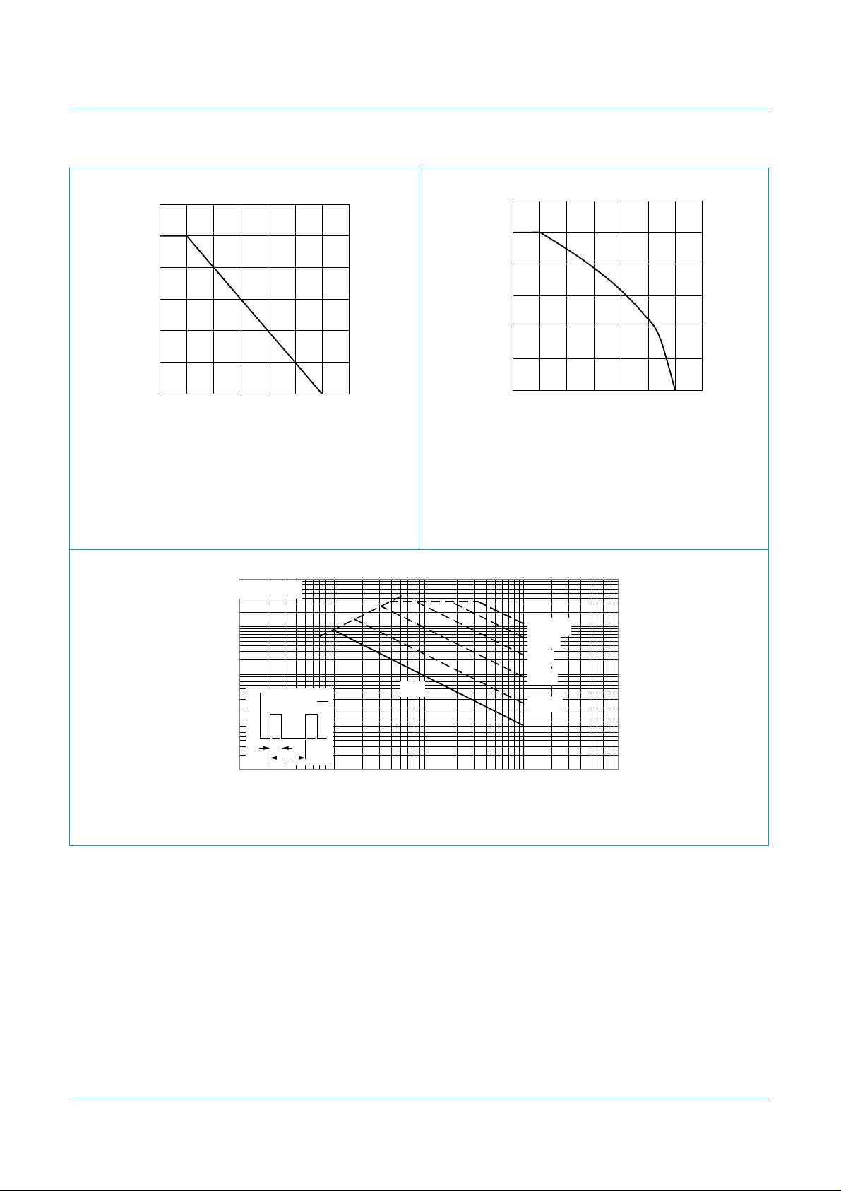
120
P
der
(%)
100
80
60
40
20
0
0 25 50 75 100 125 150 175
P
P
der
tot
----------------------
P
tot 25 C°()
100%×=
03aa17
Tsp (oC)
Fig 1. Normalized total power dissipation as a
function of solder point temperature.
10
R
= VDS/ I
(A)
1
10
10
10
DSon
I
D
-1
P
-2
-3
-1
10
D
t
p
δ =
T
t
p
t
T
1 10
120
I
der
(%)
100
80
60
40
20
0
0 25 50 75 100 125 150 175
Tsp (oC)
VGS≥ 10 V
I
D
D
------------------ -
I
D25C°()
100%×=
I
Fig 2. Normalized continuous drain current as a
function of solder point temperature.
03ac55
tp = 10 µs
100 µs
1 ms
10
10 ms
100 ms
2
VDS (V)
10
3
D.C.
03aa25
Tsp=25°C; IDM is single pulse
Fig 3. Safe operating area; drain and peak currents as a function of drain source voltage.
9397 750 07708
Product specification Rev. 01 — 09 November 2000 3 of 13
© Philips Electronics N.V. 2000. All rights reserved.
Philips Semiconductors
BSH114
N-channel enhancement mode field effect transistor
7. Thermal characteristics
Table 4: Thermal characteristics
Symbol Parameter Conditions Value Unit
R
th(j-sp)
R
th(j-amb)
thermal resistance from junction to solder point mounted on a metal clad substrate; Figure 4 150 K/W
thermal resistance from junction to ambient mounted on a printed circuit board;
350 K/W
minimum footprint
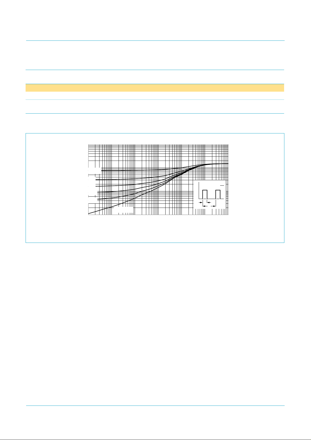
7.1 Transient thermal impedance
10
Z
th(j-sp)
(K/W)
10
10
1
3
2
δ = 0.5
0.2
0.1
0.05
0.02
single pulse
-5
10
-4
10
-3
10
-2
10
10
P
t
-1
1 10
03ac54
t
p
δ =
T
p
t
T
(s)
t
p
Tsp=25°C
Fig 4. Transient thermal impedance from junction to solder point as a function of pulse duration.
9397 750 07708
© Philips Electronics N.V. 2000. All rights reserved.
Product specification Rev. 01 — 09 November 2000 4 of 13
 Loading...