

Philips BSH105 Datasheet
Philips Semiconductors Product specification
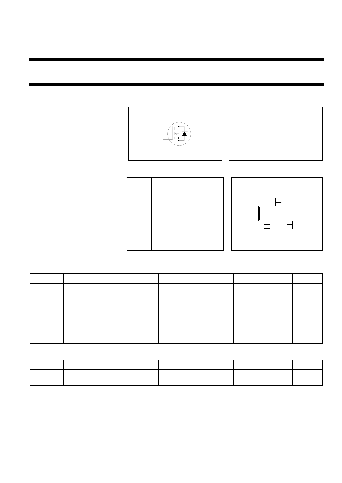
N-channel enhancement mode BSH105
MOS transistor
FEATURES SYMBOL QUICK REFERENCE DATA
• Very low threshold voltage VDS = 20 V
d
• Fast switching
• Logic level compatible ID = 1.05 A
• Subminiature surface mount
package R
g
s
≤ 250 mΩ (VGS = 2.5 V)
DS(ON)
V
≥ 0.4 V
GS(TO)
GENERAL DESCRIPTION PINNING SOT23
N-channel, enhancement mode, PIN DESCRIPTION
logic level, field-effect power
transistor. This device has very low 1 gate
3
threshold voltage and extremely
fast switching making it ideal for 2 source
battery powered applications and
high speed digital interfacing. 3 drain
The BSH105 is supplied in the
1
SOT23 subminiature surface
mounting package.
LIMITING VALUES
Limiting values in accordance with the Absolute Maximum System (IEC 134)
Top view
2
SYMBOL PARAMETER CONDITIONS MIN. MAX. UNIT
V
DS
V
DGR
V
GS
I
D
Drain-source voltage - 20 V
Drain-gate voltage RGS = 20 kΩ -20V
Gate-source voltage - ± 8V
Drain current (DC) Ta = 25 ˚C - 1.05 A
Ta = 100 ˚C - 0.67 A
I
DM
P
tot
Drain current (pulse peak value) Ta = 25 ˚C - 4.2 A
Total power dissipation Ta = 25 ˚C - 0.417 W
Ta = 100 ˚C - 0.17 W
T
stg
, T
j
Storage & operating temperature - 55 150 ˚C
THERMAL RESISTANCES
SYMBOL PARAMETER CONDITIONS TYP. MAX. UNIT
R
th j-a
Thermal resistance junction to FR4 board, minimum 300 - K/W
ambient footprint
August 1998 1 Rev 1.000

Philips Semiconductors Product specification
N-channel enhancement mode BSH105
MOS transistor
ELECTRICAL CHARACTERISTICS
Tj= 25˚C unless otherwise specified
SYMBOL PARAMETER CONDITIONS MIN. TYP. MAX. UNIT
V
(BR)DSS
V
GS(TO)
R
DS(ON)
g
fs
I
GSS
I
DSS
Q
g(tot)
Q
gs
Q
gd
t
d on
t
r
t
d off
t
f
C
iss
C
oss
C
rss
Drain-source breakdown VGS = 0 V; ID = 10 µA20--V
voltage
Gate threshold voltage VDS = VGS; ID = 1 mA 0.4 0.57 - V
Tj = 150˚C 0.1 - - V
Drain-source on-state VGS = 4.5 V; ID = 0.6 A - 140 200 mΩ
resistance VGS = 2.5 V; ID = 0.6 A - 180 250 mΩ
VGS = 1.8 V; ID = 0.3 A - 240 300 mΩ
VGS = 2.5 V; ID = 0.6 A; Tj = 150˚C - 270 375 mΩ
Forward transconductance VDS = 16 V; ID = 0.6 A 0.5 1.6 - S
Gate source leakage current VGS = ±8 V; VDS = 0 V - 10 100 nA
Zero gate voltage drain VDS = 16 V; VGS = 0 V; - 50 100 nA
current Tj = 150˚C - 1.3 10 µA
Total gate charge ID = 1 A; V
= 20 V; VGS = 4.5 V - 3.9 - nC
DD
Gate-source charge - 0.4 - nC
Gate-drain (Miller) charge - 1.4 - nC
Turn-on delay time VDD = 20 V; ID = 1 A; - 2 - ns
Turn-on rise time VGS = 8 V; RG = 6 Ω - 4.5 - ns
Turn-off delay time Resistive load - 45 - ns
Turn-off fall time - 20 - ns
Input capacitance VGS = 0 V; VDS = 16 V; f = 1 MHz - 152 - pF
Output capacitance - 71 - pF
Feedback capacitance - 33 - pF
REVERSE DIODE LIMITING VALUES AND CHARACTERISTICS
Tj = 25˚C unless otherwise specified
SYMBOL PARAMETER CONDITIONS MIN. TYP. MAX. UNIT
I
DR
I
DRM
V
t
rr
Q
SD
rr
Continuous reverse drain Ta = 25 ˚C - - 1.05 A
current
Pulsed reverse drain current - - 4.2 A
Diode forward voltage IF = 0.5 A; VGS = 0 V - 0.74 1 V
Reverse recovery time IF = 0.5 A; -dIF/dt = 100 A/µs; - 27 - ns
Reverse recovery charge VGS = 0 V; VR = 16 V - 19 - nC
August 1998 2 Rev 1.000
Philips Semiconductors Product specification
N-channel enhancement mode BSH105
MOS transistor
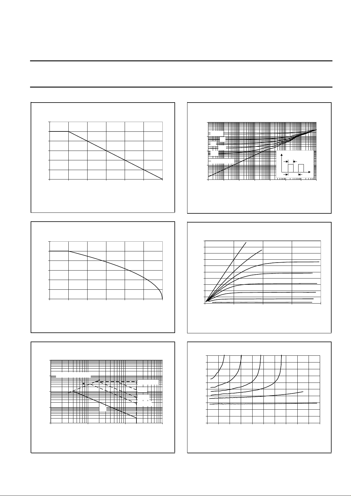
Normalised Power Dissipation, PD (%)
120
100
80
60
40
20
0
0 25 50 75 100 125 150
Ambient Temperature, Ta (C)
Fig.1. Normalised power dissipation.
PD% = 100⋅PD/P
Normalised Drain Current, ID (%)
120
100
80
60
40
20
0
0 25 50 75 100 125 150
Ambient Temperature, Ta (C)
D 25 ˚C
= f(Ta)
Fig.2. Normalised continuous drain current.
ID% = 100⋅ID/I
= f(Ta); conditions: VGS ≥ 4.5 V
D 25 ˚C
Peak Pulsed Drain Current, IDM (A)
1000
D = 0.5
100
10
0.1
0.2
0.1
0.05
0.02
single pulse
1
1E-06 1E-05 1E-04 1E-03 1E-02 1E-01 1E+00 1E+01
Pulse width, tp (s)
P
D
tp
T
BSH105
D = tp/T
Fig.4. Transient thermal impedance.
Z
= f(t); parameter D = tp/T
th j-a
Drain Current, ID (A)
5
4.5
4
Tj = 25 C
3.5
3
2.5
2
1.5
1
0.5
0
0 0.5 1 1.5 2
4.5V
2.5V
Drain-Source Voltage, VDS (V)
BSH105
2.1 V
VGS = 1.9 V
1.7 V
1.5 V
1.3 V
1.1 V
Fig.5. Typical output characteristics, Tj = 25 ˚C
ID = f(VDS); parameter V
GS
.
Peak Pulsed Drain Current, IDM (A)
100
RDS(on) = VDS/ ID
10
1
0.1
0.01
0.1 1 10 100
Drain-Source Voltage, VDS (V)
d.c.
BSH105
tp = 100 us
1 ms
10 ms
100 ms
Fig.3. Safe operating area. Ta = 25 ˚C
ID & IDM = f(VDS); IDM single pulse; parameter t
Drain-Source On Resistance, RDS(on) (Ohms)
0.5
0.45
0.4
0.35
0.3
0.25
0.2
0.15
0.1
0.05
Tj = 25 C
0
0 0.5 1 1.5 2 2.5 3 3.5 4 4.5 5
1.7 V
1.5 V
Drain Current, ID (A)
1.9 V
2.1 V
Fig.6. Typical on-state resistance, Tj = 25 ˚C
R
p
= f(ID); parameter V
DS(ON)
BSH105
2.5 V
VGS = 4.5 V
.
GS
August 1998 3 Rev 1.000
 Loading...