

Philips BSH104 Datasheet

DISCRETE SEMICONDUCTORS
DATA SH EET
ook, halfpage
M3D088
BSH104
N-channel enhancement mode
MOS transistor
Objective specification
File under Discrete Semiconductors, SC13b
1997 Nov 26
Philips Semiconductors Objective specification
N-channel enhancement mode
MOS transistor
FEATURES
• High-speed switching
• No secondary breakdown
• Direct interface to C-MOS, TTL, etc.
• Very low threshold.
APPLICATIONS
• ‘Glue-logic’: interface between logic blocks and/or
periphery
• Power management
• DC to DC converters
• General purpose switch
• Battery powered applications.
DESCRIPTION
N-channel enhancement mode MOS transistor in a SOT23
SMD package.
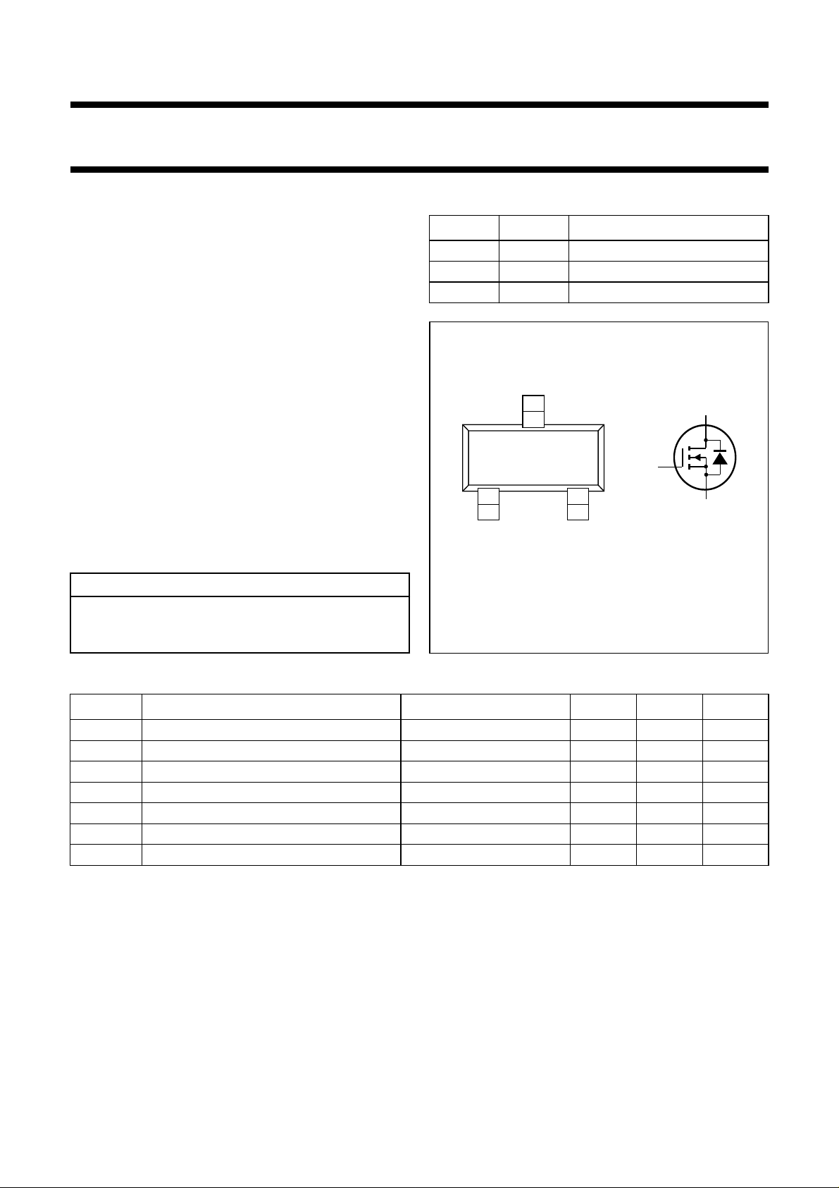
PINNING
PIN SYMBOL DESCRIPTION
1 g gate
2 s source
3 d drain
handbook, halfpage
Top view
3
g
21
MAM273
BSH104
d
s
CAUTION
The device is supplied in an antistatic package.
The gate-source input must be protected against static
Fig.1 Simplified outline (SOT23) and symbol.
discharge during transport or handling.
QUICK REFERENCE DATA
SYMBOL PARAMETER CONDITIONS MIN. MAX. UNIT
V
DS
V
SD
V
GS
V
GSth
I
D
R
DSon
P
tot
drain-source voltage (DC) − 12 V
source-drain diode forward voltage VGD= 0; IS= 0.5 A − 1V
gate-source voltage (DC) −±8V
gate-source threshold voltage VDS=VGS; ID=1mA 0.4 − V
drain current (DC) Ts=80°C − 1.1 A
drain-source on-state resistance VGS= 2.5 V; ID= 0.65 A − 0.3 Ω
total power dissipation Ts=80°C − 0.5 W
1997 Nov 26 2

Philips Semiconductors Objective specification
N-channel enhancement mode
BSH104
MOS transistor
LIMITING VALUES
In accordance with the Absolute Maximum Rating System (IEC 134).
SYMBOL PARAMETER CONDITIONS MIN. MAX. UNIT
V
DS
V
GS
I
D
I
DM
P
tot
T
stg
T
j
Source-drain diode
I
S
I
SM
Notes
1. T
s
2. Pulse width and duty cycle limited by maximum junction temperature.
3. Device mounted on a printed-circuit board with a R
4. Device mounted on a printed-circuit board with a R
drain-source voltage (DC) − 12 V
gate-source voltage (DC) −±8V
drain current (DC) Ts=80°C; note 1 − 1.1 A
peak drain current note 2 − 4.5 A
total power dissipation Ts=80°C − 0.5 W
T
=25°C; note 3 − 0.75 W
amb
T
=25°C; note 4 − 0.54 W
amb
storage temperature −55 +150 °C
operating junction temperature −55 +150 °C
source current (DC) Ts=80°C − 0.5 A
peak pulsed source current note 2 − 2A
is the temperature at the soldering point of the drain lead.
(ambient to tie-point) of 27.5 K/W.
th a-tp
(ambient to tie-point) of 90 K/W.
th a-tp
THERMAL CHARACTERISTICS
SYMBOL PARAMETER VALUE UNIT
R
th j-s
thermal resistance from junction to soldering point 140 K/W
1997 Nov 26 3
 Loading...