

Philips BRY62 Datasheet

DISCRETE SEMICONDUCTORS
DATA SH EET
M3D071
BRY62
Silicon controlled switch
Product specification
Supersedes data of 1997 Jul 21
1999 Apr 22

Philips Semiconductors Product specification
Silicon controlled switch BRY62
DESCRIPTION
Silicon planar PNPN switch in a
SOT143B plastic package. It is an
integrated PNP/NPN transistor pair,
with all electrodes accessible.
PINNING
PIN DESCRIPTION
1 anode gate
2 anode
3 cathode
APPLICATIONS
4 cathode gate
• Switching applications.
MARKING
TYPE
NUMBER
MARKING
CODE
BRY62 A51
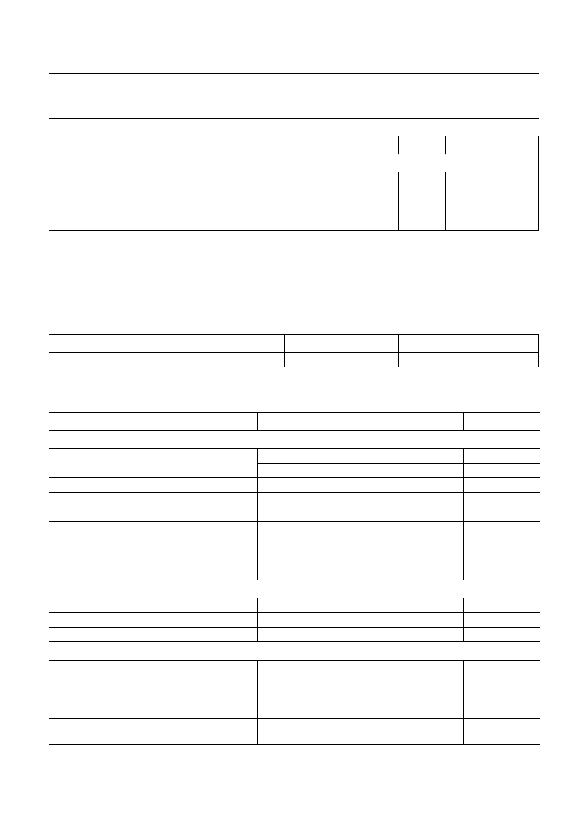
handbook, 2 columns
12
Top view
Fig.1 Simplified outline (SOT143B) and symbol.
LIMITING VALUES
In accordance with the Absolute Maximum Rating System (IEC 134).
34
MSB014
a
ag
kg
MBB068
k
SYMBOL PARAMETER CONDITIONS MIN. MAX. UNIT
NPN transistor
V
CBO
V
CER
V
EBO
I
C
I
CM
I
E
I
ERM
collector-base voltage open emitter − 70 V
collector-emitter voltage RBE=10kΩ−70 V
emitter-base voltage open collector − 5V
collector current (DC) note 1 − 175 mA
peak collector current note 2 − 175 mA
emitter current (DC) −−175 mA
repetitive peak emitter current tp=10µs; δ = 0.01 −−2.5 A
PNP transistor
V
V
V
I
E
I
ERM
CBO
CEO
EBO
collector-base voltage open emitter −−70 V
collector-emitter voltage open base −−70 V
emitter-base voltage open collector −−70 V
emitter current (DC) − 175 mA
repetitive peak emitter current tp=10µs; δ = 0.01 − 2.5 A
1999 Apr 22 2
Philips Semiconductors Product specification
Silicon controlled switch BRY62
SYMBOL PARAMETER CONDITIONS MIN. MAX. UNIT
Combined device
P
tot
T
stg
T
j
T
amb
total power dissipation T
storage temperature −65 +150 °C
junction temperature − 150 °C
operating ambient temperature see Fig.14 −65 +150 °C
Notes
1. Provided the IE rating is not exceeded.
2. During switching on, the device can withstand the discharge of a capacitor of a maximum value of 500 pF. This
capacitor is charged when the transistor is in cut-off condition, with a collector supply voltage of 160 V and a series
resistance of 100 kΩ.
THERMAL CHARACTERISTICS
SYMBOL PARAMETER CONDITIONS VALUE UNIT
R
th j-a
thermal resistance from junction to ambient in free air 500 K/W
≤ 25 °C − 250 mW
amb
CHARACTERISTICS
=25°C unless otherwise specified.
T
amb
SYMBOL PARAMETER CONDITIONS MIN. MAX. UNIT
NPN transistor
I
CER
I
EBO
V
CEsat
V
BEsat
h
FE
f
T
C
c
C
e
collector cut-off current VCE=70V; RBE=10kΩ−100 nA
=70V; RBE=10kΩ; Tj= 150 °C − 10 µA
V
CE
emitter cut-off current IC= 0; VEB=5V; Tj= 150 °C − 10 µA
collector-emitter saturation voltage IC= 10 mA; IB=1mA − 500 mV
base-emitter saturation voltage IC= 10 mA; IB=1mA − 900 mV
DC current gain IC= 10 mA; VCE=2V 50 −
transition frequency IC= 10 mA; VCE= 2 V; f = 100 MHz 100 − MHz
collector capacitance IE=ie= 0; VCB= 20 V; f = 1 MHz − 5pF
emitter capacitance IC=ic= 0; VEB= 1 V; f = 1 MHz − 25 pF
PNP transistor
I
CEO
I
EBO
h
FE
collector cut-off current IB= 0; VCE= −70 V; Tj= 150 °C −−10 µA
emitter cut-off current IC= 0; VEB= −70 V; Tj= 150 °C −−10 µA
DC current gain IE= 1 mA; VCB= −5V 3 15
Combined device
V
AK
I
H
forward on-state voltage R
holding current R
=10kΩ
KG-K
= 50 mA; IAG=0 − 1.4 V
I
A
= 50 mA; IAG= 0; Tj= − 55 °C − 1.9 V
I
A
I
= 1 mA; IAG=10mA − 1.2 V
A
=10kΩ;IAG= 10 mA;
KG-K
− 1mA
VBB= −2 V; (see Fig.5)
1999 Apr 22 3
Philips Semiconductors Product specification
Silicon controlled switch BRY62
SYMBOL PARAMETER CONDITIONS MIN. MAX. UNIT
Switching times
t
on
t
off
turn-on time V
turn-off time R
a (anode)
(e )
2
PNP transistor
kg (cathode gate)
(b ,c )
12
k (cathode)
(e )
ag (anode gate)
(c ,b )
NPN transistor
1
12
MBB680
= −0.5 to 4.5 V; R
KG-K
KG-K
=1kΩ;
− 0.25 µs
see Figs 6 and 7
V
= −0.5 to 0.5 V; R
KG-K
=10kΩ; see Figs 8 and 9 − 15 µs
KG-K
handbook, halfpage
=10kΩ− 1.5 µs
KG-K
e
2
P
b ,c
12
N
P
N
P
N
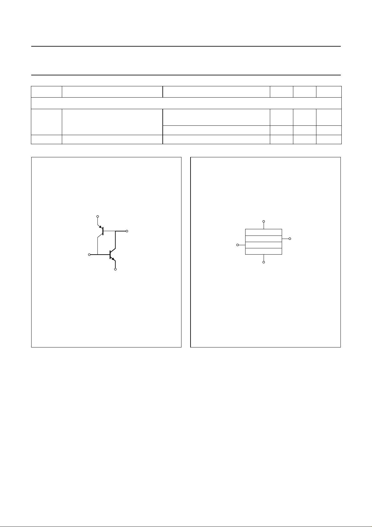
MBB681
e
1
c ,b
12
Fig.2 Two transistor equivalent circuit.
1999 Apr 22 4
Fig.3 PNPN silicon controlled switch structure.
 Loading...