

Philips bry56 DATASHEETS

DISCRETE SEMICONDUCTORS
DATA SH EET
ook, halfpage
M3D186
BRY56
Programmable unijunction
transistor
Product specification
Supersedes data of September 1994
File under Discrete Semiconductors, SC04
1997 Jul 21
Philips Semiconductors Product specification
Programmable unijunction transistor BRY56
DESCRIPTION
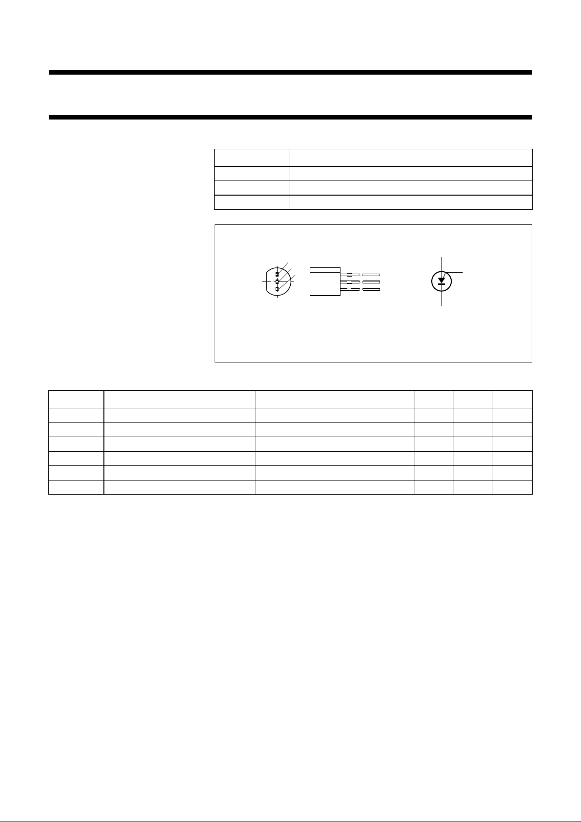
Planar PNPN trigger device in a
TO-92; SOT54 plastic package.
PINNING
PIN DESCRIPTION
1 gate
2 anode
APPLICATIONS
3 cathode
• Switching applications such as:
– Motor control
– Oscillators
– Relay replacement
– Timers
handbook, halfpage
1
2
3
anode
a
g
gate
– Pulse shapers, etc.
MSB033
k
cathode
MGL167
Fig.1 Simplified outline (TO-92; SOT54) and symbol.
QUICK REFERENCE DATA
SYMBOL PARAMETER CONDITIONS MIN. MAX. UNIT
V
GA
I
A(AV)
P
tot
T
j
I
P
I
V
gate-anode voltage − 70 V
average anode current − 175 mA
total power dissipation T
≤ 75 °C − 300 mW
amb
operating junction temperature − 150 °C
peak point current VS= 10 V; RG=10kΩ−0.2 µA
valley point current VS= 10 V; RG=10kΩ 2 −µA
1997 Jul 21 2

Philips Semiconductors Product specification
Programmable unijunction transistor BRY56
LIMITING VALUES
In accordance with the Absolute Maximum Rating System (IEC 134).
SYMBOL PARAMETER CONDITIONS MIN. MAX. UNIT
V
GA
I
A(AV)
I
ARM
I
ASM
/dt rate of rise of anode current IA≤ 2.5 A − 20 A/µs
dl
A
P
tot
T
stg
T
j
T
amb
THERMAL CHARACTERISTICS
gate-anode voltage − 70 V
average anode current − 175 mA
repetitive peak anode current tp=10µs; δ = 0.01 − 2.5 A
non-repetitive peak anode current tp=10µs − 3A
total power dissipation T
≤ 75 °C − 300 mW
amb
storage temperature −65 +150 °C
junction temperature − 150 °C
operating ambient temperature −65 +150 °C
SYMBOL PARAMETER CONDITIONS VALUE UNIT
R
th j-a
thermal resistance from junction to ambient in free air 250 K/W
CHARACTERISTICS
=25°C unless otherwise specified.
T
amb
SYMBOL PARAMETER CONDITIONS MIN. TYP. MAX. UNIT
I
P
I
V
V
offset
I
GAO
I
GKS
V
AK
V
OM
peak point current VS= 10 V; RG=10kΩ; see Fig.7 −−200 nA
V
= 10 V; RG= 100 kΩ; see Fig.7 −−60 nA
S
valley point current VS= 10 V; RG=10kΩ; see Fig.7 2 −−µA
V
= 10 V; RG= 100 kΩ; see Fig.7 1 −−µA
S
offset voltage typical curve; IA= 0; see Fig.7 − VP−VS− V
gate-anode leakage current IK= 0; VGA= 70 V; see Fig.5 −−10 nA
gate-cathode leakage current VAK= 0; VKG= 70 V; see Fig.6 −−100 nA
anode-cathode voltage IA= 100 mA −−1.4 V
peak output voltage VAA= 20 V; C = 10 nF;
6 −−V
see Figs 8 and 9
t
r
rise time VAA= 20 V; C = 10 nF; see Fig.9 −−80 ns
1997 Jul 21 3
Philips Semiconductors Product specification
Programmable unijunction transistor BRY56
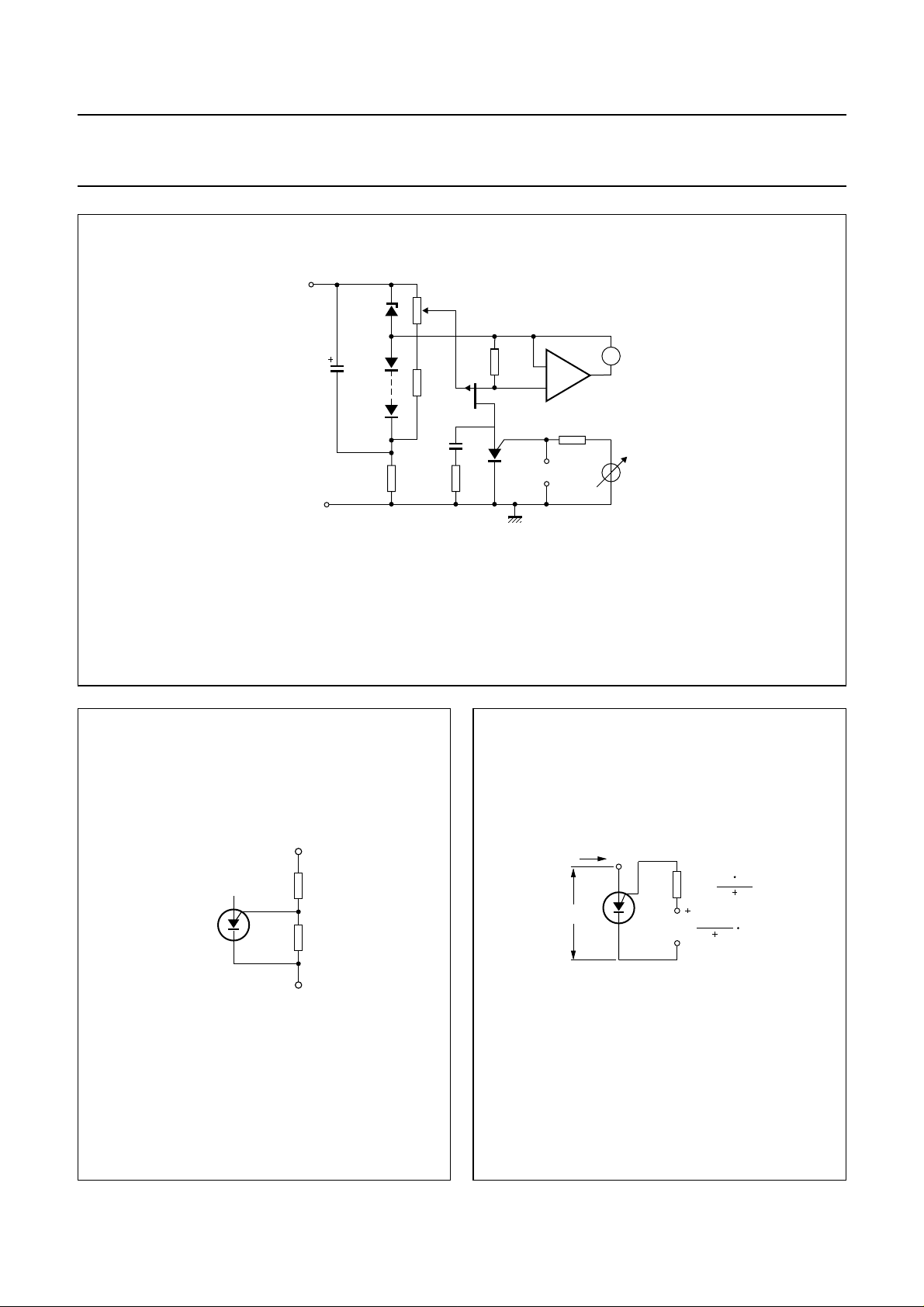
handbook, full pagewidth
IP and IV determined by value of R1.
1
; i.e. maximum voltage drop over R1 =1 V.
R1
=
---I
A
Internal resistance of oscilloscope = 10 MΩ.
+40 V
100 µF
Fig.2 Measuring circuit for peak and valley point currents.
BZY88-
C8V2
BY206
(2x)
5 kΩ
750
Ω
1 nF
20 Ω10 kΩ
R1
D.U.T
osc.
40 K
R
G
MBK189
A
V
S
handbook, halfpage
DUT
MEA141
+V
B
R2
R1
Fig.3 BRY56 with ‘program’ resistors R1 and R2.
1997 Jul 21 4
handbook, halfpage
I
A
R1R
RG =
R1R
V
AK
DUT
MBB699
VS =
R
1
V
R
R
2
1
Fig.4 Equivalent test circuit for
characteristics testing.
2
2
B
 Loading...