

Philips brs212 DATASHEETS
Philips Semiconductors Product specification
Breakover diodes BRS212 series
GENERAL DESCRIPTION QUICK REFERENCE DATA
A range of bidirectional, breakover SYMBOL PARAMETER MIN. TYP. MAX. UNIT diodes in a two terminal, surface mounting, plastic envelope. These V devices feature controlled breakover BRS212-140 - 140 - V
(BO)
voltage and high holding current BRS212-160 - 160 - V
together with high peak current BRS212-180 - 180 - V
handling capability. Their intended BRS212-200 - 200 - V
application isprotection of line based BRS212-220 - 220 - V
telecommunications equipment BRS212-240 - 240 - V
against voltage transients. BRS212-260 - 260 - V
I
H
I
PP
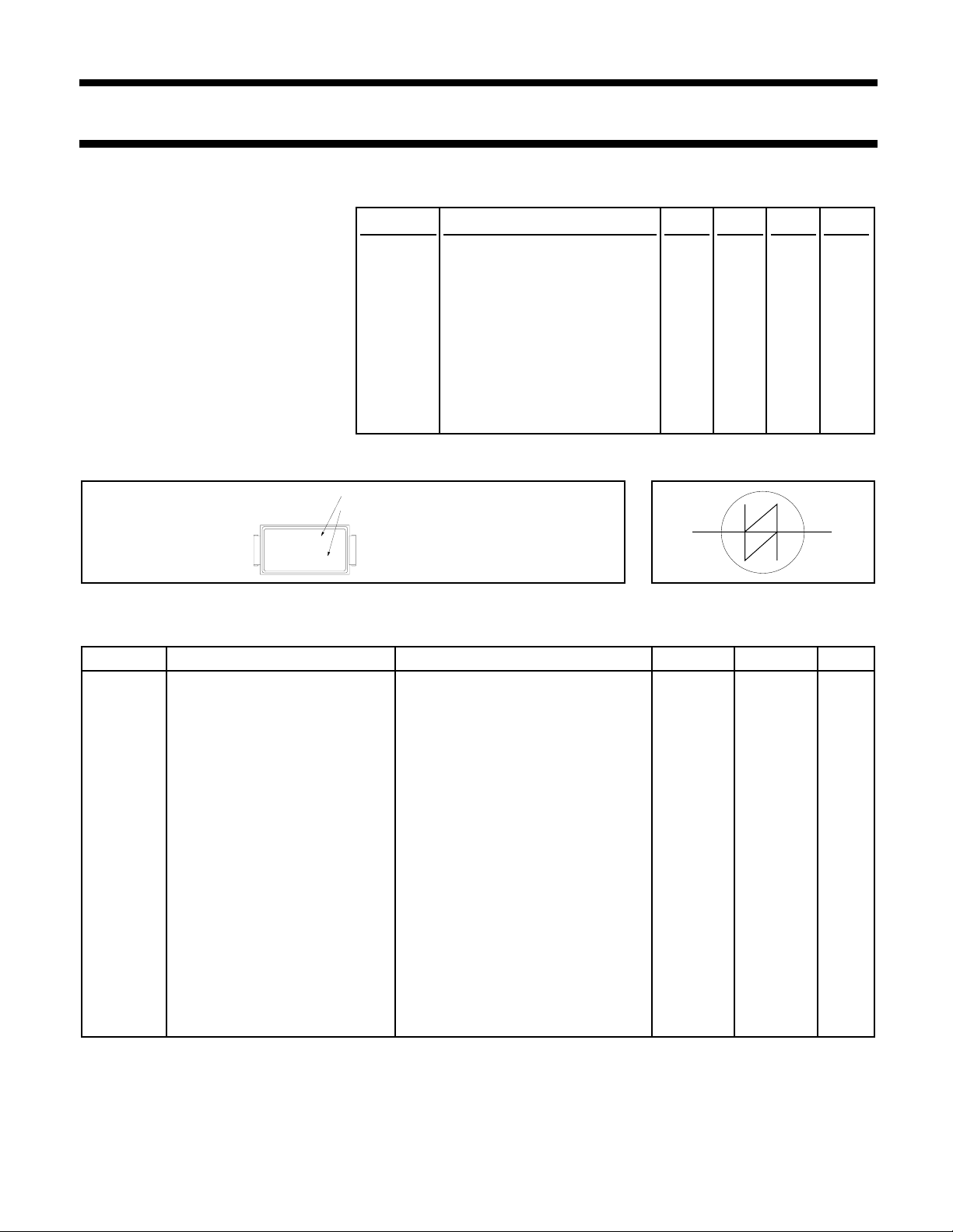
OUTLINE - SOD106 SYMBOL
date code
XXX denotes voltage grade
Breakover voltage
BRS212-280 - 280 - V
Holding current 150 - - mA
Non-repetitive peak pulse - - 40 A
current (CCITT K17)
YM
212
PH
XXX
LIMITING VALUES
Limiting values in accordance with the Absolute Maximum System (IEC 134).
SYMBOL PARAMETER CONDITIONS MIN. MAX. UNIT
V
D
I
PP
I
TSM
I2tI
dIT/dt Rate of rise of on-state current tp = 10 µs - 50 A/µs
P
tot
P
TM
T
stg
T
j
T
L
Continuous voltage BRS212-140 - 105 V
BRS212-160 - 120 V
BRS212-180 - 135 V
BRS212-200 - 150 V
BRS212-220 - 165 V
BRS212-240 - 180 V
BRS212-260 - 195 V
BRS212-280 - 210 V
Non-repetitive peak pulse 5/310 µs impulse equivalent to - 40 A
current 10/700 µs, 1.6 kV voltage impulse
(CCITT K17)
Non repetitive surge peak half sine wave; t = 10 ms; - 15 A
on-state current Tj = 70 ˚C prior to surge
2
t for fusing tp = 10 ms - 1.1 A2s
after V
Continuous dissipation on Tsp = 50˚C - 4 W
turn-on
(BO)
infinite heatsink
Peak dissipation tp = 1 ms; Ta = 25˚C - 50 W
Storage temperature - 40 150 ˚C
Operating junction temperature - 150 ˚C
Maximum terminal temperature soldering time = 10 s - 260 ˚C
for soldering
January 1997 1 Rev 1.000

Philips Semiconductors Product specification
Breakover diodes BRS212 series
THERMAL RESISTANCES
SYMBOL PARAMETER CONDITIONS MIN. TYP. MAX. UNIT
R
th j-sp
R
th j-a
Z
th j-a
ELECTRICAL CHARACTERISTICS
Tj = 25 ˚C unless otherwise stated
TYPE PARAMETER
Conditions IBR = 10 mA ID ≤ I
BRS212-140 212-140 123 140 140 157 10 105 2000 105
BRS212-160 212-160 140 160 160 180 10 120 2000 120
BRS212-180 212-180 158 180 180 202 10 135 2000 135
BRS212-200 212-200 176 200 200 224 10 150 2000 150
BRS212-220 212-220 193 220 220 247 10 165 2000 165
BRS212-240 212-240 211 240 240 269 10 180 2000 180
BRS212-260 212-260 228 260 260 292 10 195 2000 195
BRS212-280 212-280 246 280 280 314 10 210 2000 210
Thermal resistance junction to - - 25 K/W
solder point
Thermal resistance junction to pcb mounted; minimum footprint - 100 - K/W
ambient
Thermal impedance junction to tp = 1 ms - 2.6 - K/W
ambient
Marking Avalanche Breakover Off-state current Critical rate of
voltage voltage rise of off-state
voltage
Tj = 70˚C; Tj = 70˚C
ID @ V
D
dVD/dt @ V
DM
Symbol V
BR
tp = 100 µs RH ≤ 65%
S
V
BO
Limits min typ typ max max max
Units VVVVµAVV/µsV
SYMBOL PARAMETER CONDITIONS MIN. TYP. MAX. UNIT
V
T
I
H
I
S
S
(BR)
C
j
On-state voltage ITM = 2 A; tp = 200 µs - - 2.5 V
Holding current
Switching current
1
2
Tj = 25˚C 150 - - mA
Tj = 70˚C 100 - - mA
tp = 100 µs 10 200 1000 mA
Temperature coefficient of - +0.1 - %/K
avalanche voltage
Junction capacitance VD = 0 V, f = 1 kHz to 1 MHz - - 100 pF
1 The minimum current at which the diode will remain in the on-state
2 The avalanche current required to switch the diode to the on-state.
January 1997 2 Rev 1.000
 Loading...