

Philips BR101 Datasheet
DISCRETE SEMICONDUCTORS
DATA SH EET
M3D082
BR101
Silicon controlled switch
Product specification
Supersedes data of September 1994
File under Discrete Semiconductors, SC04
1997 Jul 24

Philips Semiconductors Product specification
Silicon controlled switch BR101
DESCRIPTION
Silicon planar PNPN switch in a
TO-72 metal package. It is an
integrated PNP/NPN transistor pair,
with all electrodes accessible.
APPLICATIONS
• Time base circuits
• Switching in television circuits
• Trigger device for thyristors.
PINNING
PIN DESCRIPTION
k, halfpage
1 cathode
2 cathode gate
3 anode gate (connected to case)
4 anode
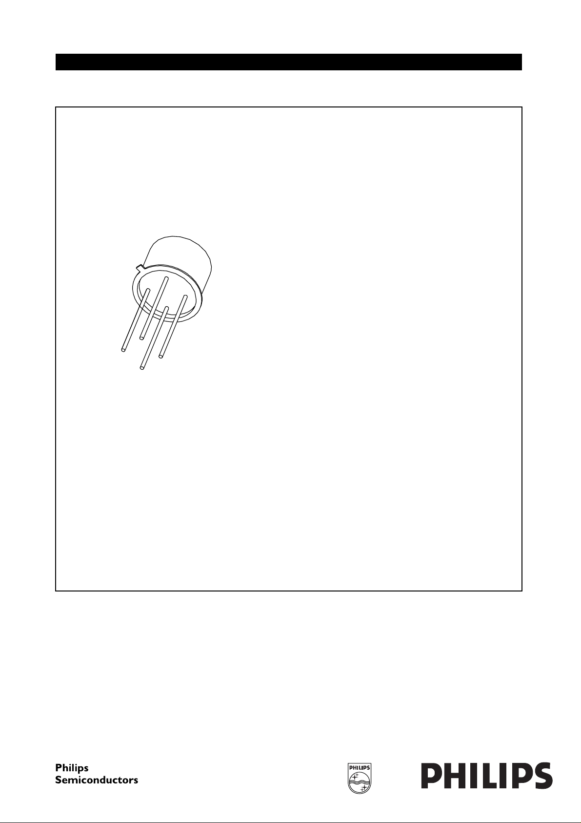
handbook, halfpage
1
2
4
3
MSB028
Fig.1 Simplified outline (TO-72) and symbol.
a
ag
kg
k
MGL168
QUICK REFERENCE DATA
SYMBOL PARAMETER CONDITIONS MAX. UNIT
PNP transistor
V
EBO
emitter-base voltage open collector −50 V
NPN transistor
V
I
ERM
P
T
V
I
H
CBO
tot
j
AK
collector-base voltage open emitter 50 V
repetitive peak emitter current −2.5 A
total power dissipation T
≤ 25 °C 275 mW
amb
junction temperature 150 °C
forward on-state voltage IA= 50 mA; IAG= 0; R
holding current IAG= 10 mA; VBB= −2 V; R
=10kΩ 1.4 V
KG-K
=10kΩ 1mA
KG-K
1997 Jul 24 2

Philips Semiconductors Product specification
Silicon controlled switch BR101
LIMITING VALUES
In accordance with the Absolute Maximum Rating System (IEC 134).
SYMBOL PARAMETER CONDITIONS MIN. MAX. UNIT
NPN transistor
V
CBO
V
CER
V
EBO
I
C
I
CM
I
E
I
ERM
PNP transistor
V
CBO
V
CEO
V
EBO
I
E
I
ERM
Combined device
P
tot
T
stg
T
j
T
amb
collector-base voltage open emitter − 50 V
collector-emitter voltage RBE=10kΩ−50 V
emitter-base voltage open collector; note 1 − 5V
collector current (DC) note 2 − 175 mA
peak collector current − 175 mA
emitter current (DC) −−175 mA
repetitive peak emitter current tp=10µs; δ = 0.01 −−2.5 A
collector-base voltage open emitter −−50 V
collector-emitter voltage open base −−50 V
emitter-base voltage open collector −−50 V
emitter current (DC) − 175 mA
repetitive peak emitter current tp=10µs; δ = 0.01 − 2.5 A
total power dissipation T
≤ 25 °C − 275 mW
amb
storage temperature −65 +150 °C
junction temperature − 150 °C
operating ambient temperature −65 +150 °C
Notes
1. It is permitted to exceed this voltage during the discharge of a capacitor of max. 390 pF, provided the charge does
not exceed 50 nC.
2. Provided the I
rating is not exceeded.
E
THERMAL CHARACTERISTICS
SYMBOL PARAMETER CONDITIONS VALUE UNIT
R
th j-a
thermal resistance from junction to ambient in free air 0.45 K/mW
1997 Jul 24 3
 Loading...