

Philips BP2.1U, BP2.2U, BP2.3U Service Manual
Color Television Chassis
BP2.1U, BP2.2U, BP2.3U
AA
Service Manual SDI Plasma Panels: 3122 785 14990
F_15400_000.eps
200505
Contents Page Contents Page
1. Technical Specifications, Connections, and Chassis
Overview 2
2. Safety Instructions, Warnings, and Notes 5
3. Directions for Use 7
4. Mechanical Instructions 8
5. Service Modes, Error Codes, and Fault Finding 13
6. Block Diagrams and Overviews
Wiring Diagram 33
Block Diagram Video 34
Block Diagram Audio 35
Block Diagram Control 36
I2C ICs Overview 37
Supply Lines Overview 38
7. Circuit Diagrams and PWB Layouts Drawing PWB
Ambi Light Panel (Optional) (AL) 39 40
SSB: DC/DC (B1A) 41 80-89
SSB: DC/DC Connections (B1B) 42 80-89
SSB: RS232 Interface (B1C) 43 80-89
SSB: Channel Decoder (B2A) 44 80-89
SSB: Main Tuner & OOB Tuner (B2B) 45 80-89
SSB: MPIF Main: Video Source Selection (B3A) 46 80-89
SSB: MPIF Main: Supply (B3B) 47 80-89
SSB: MPIF Main: IF & SAW Filter (B3C) 48 80-89
SSB: MPIF Main: Audio Source Selection (B3D) 49 80-89
SSB: MPIF Main: Audio Amplifier (B3E) 50 80-89
SSB: MPIF Main: Connections A (B3F) 51 80-89
SSB: MPIF Main: Connections B (B3G) 52 80-89
SSB: PNX2015: Audio/Video (B4A) 53 80-89
SSB: PNX2015: DV I/O Interface (B4B) 54 80-89
SSB: PNX2015: Tunnel Bus (B4C) 55 80-89
SSB: PNX2015: DDR Interface (B4D) 56 80-89
SSB: PNX2015: Standby & Control (B4E) 57 80-89
SSB: PNX2015: Supply (B4F) 58 80-89
SSB: PNX2015: Display Interface (B4G) 59 80-89
©
Copyright 2005 Philips Consumer Electronics B.V. Eindhoven, The Netherlands.
All rights reserved. No part of this publication may be reproduced, stored in a
retrieval system or transmitted, in any form or by any means, electronic,
mechanical, photocopying, or otherwise without the prior permission of Philips.
SSB: Viper: Control (B5A) 60 80-89
SSB: Viper: Main Memory (B5B) 61 80-89
SSB: Viper: A/V & Tunnel Bus (B5C) 62 80-89
SSB: Viper: Supply (B5D) 63 80-89
SSB: Viper: Display Diversity & Ambilight (B5E) 64 80-89
SSB: Display Interface: MOP (B6) 65 80-89
SSB: HDMI (B7A) 66 80-89
SSB: HDMI: I/O & Control (B7B) 67 80-89
SSB: HDMI: Supply (B7C) 68 80-89
SSB: USB2.0: Host (Optional) (B8) 69 80-89
SSB: Ethernet (Optional) (B9A) 70 80-89
SSB: UART (B9B) 71 80-89
SSB: POD: Out of Band (B10B) 71 80-89
SSB: POD: Common Interface (B10A) 72 80-89
SSB: POD: Buffering (B10C) 73 80-89
SSB: POD: TS Buffering (B10D) 74 80-89
SSB: Firewire 1394: Main (Optional) (B11A) 75 80-89
SSB: Firewire 1394: Buffering (Optional) (B11B) 76 80-89
SSB: Miscelaneous (B12) 77 80-89
SRP Overview SSB 78-79 80-89
External I/O Panel: Externals A (BE1) 90 92
External I/O Panel: Externals B (BE2) 91 92
Audio Amplifier Panel (C) 93 94
Side I/O Panel (D) 95 96
Control Board (E) 97 98
LED Panel (J) 99 100
8. Alignments 101
9. Circuit Descriptions, Abbreviation List, and IC Data
Sheets 106
Abbreviation List 126
IC Data Sheets 129
10. Spare Parts List 142
11. Revision List 151
Published by EL 0567 TV Service Printed in the Netherlands Subject to modification EN 3122 785 15541
EN 2 BP2.1U, 2.2U, 2.3U1.
Technical Specifications, Connections, and Chassis Overview
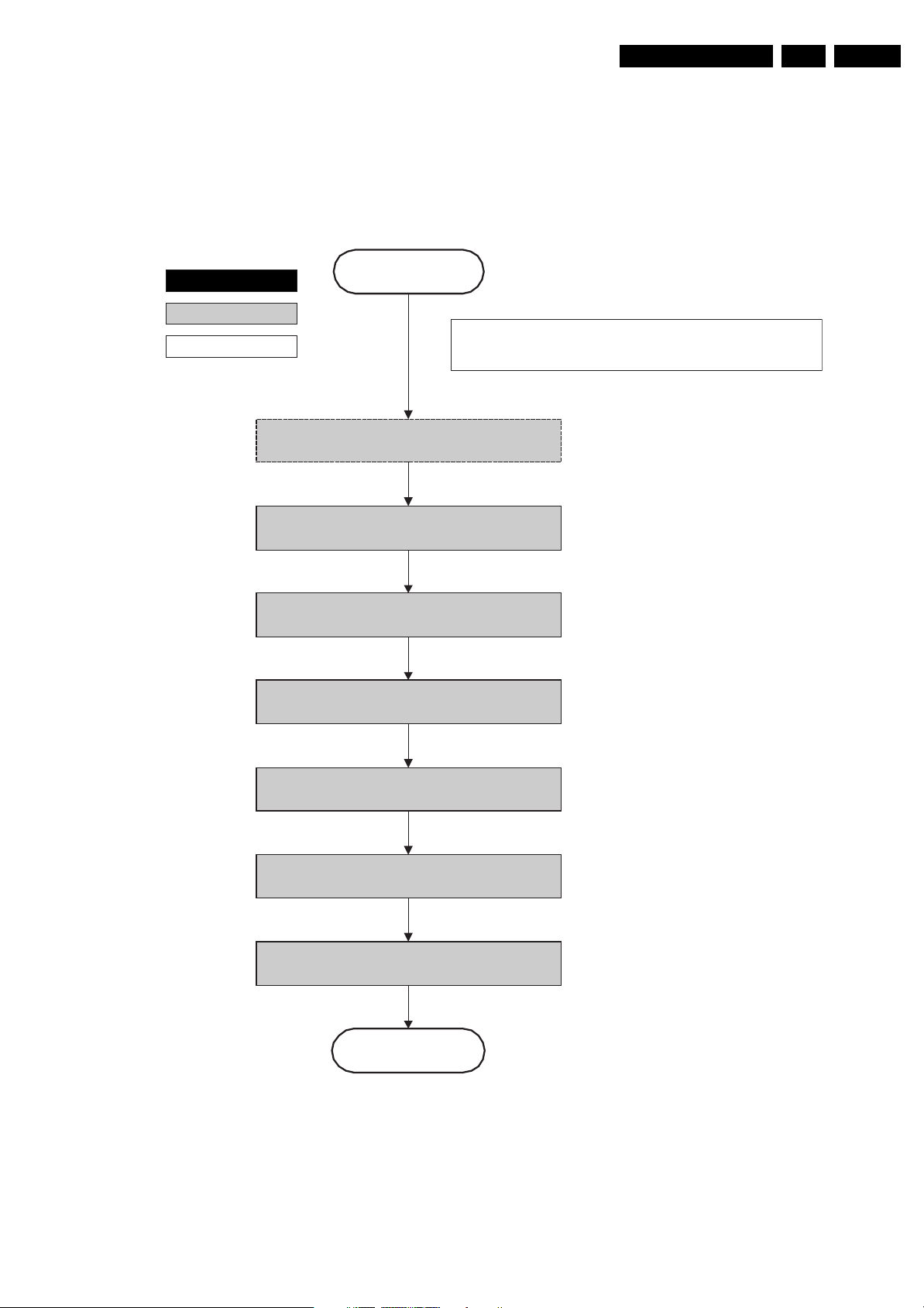
1. Technical Specifications, Connections, and Chassis Overview
Index of this chapter:
1.1 Technical Specifications
1.2 Connection Overview
1.3 Chassis Overview
Notes:
• Data below can deviate slightly from the actual situation,
due to the different set executions
• Specifications are indicative (subject to change).
1.1 Technical Specifications
1.1.1 Vision
Display type : Plasma (SDI)
Screen size : 42” (107 cm), 16:9
Resolution (HxV pixels) : 1024(*3)x768p (42”)
Min. contrast ratio : 8000:1 (42”)
Min. light output (cd/m
Viewing angle (HxV degrees) : 160x160
Tuning system : PLL
TV Color systems : ATSC
Video playback : NTSC
Cable : Unscrambled digital
Tuner bands : VHF
Supported video formats : 640x480i - 1fH
Supported computer formats : 640x480 @ 60Hz
2
) : 900
: 50” (127 cm), 16:9
: 1366(*3)x768p (50”)
: 9000:1 (50”)
:NTSC
cable - QAM
: Digital cable ready -
CableCard
: UHF
: S-band
: Hyper-band
: 640x480p - 2fH
: 720x576i - 1fH
: 720x576p - 2fH
: 1280x720p - 3fH
: 1920x1080i - 2fH
: 800x600 @ 60Hz
: 1024x768 @ 60Hz
: 1366x768 @ 60Hz
1.1.4 Miscellaneous
Power supply:
- Mains voltage (V
- Mains frequency (Hz) : 50/60
Ambient conditions:
- Temperature range (°C) : +5 to +40
- Maximum humidity : 90% R.H.
Power consumption (values are indicative)
- Normal operation (W) : ≈ 400 (42”)
- Standby (W) : < 2
Dimensions (WxHxD in cm) : 124x68x10.4 (42”)
Weight (kg/lbs) : 42/92.6 (42”)
) : 100 - 240
AC
: ≈ 467 (50”)
: 141x78x10.4 (50”)
: 60/132.3 (50”)
1.2 Connection Overview
Note: The following connector color abbreviations are used
(acc. to DIN/IEC 757): Bk= Black, Bu= Blue, Gn= Green, Gy=
Grey, Rd= Red, Wh= White, and Ye= Yellow.
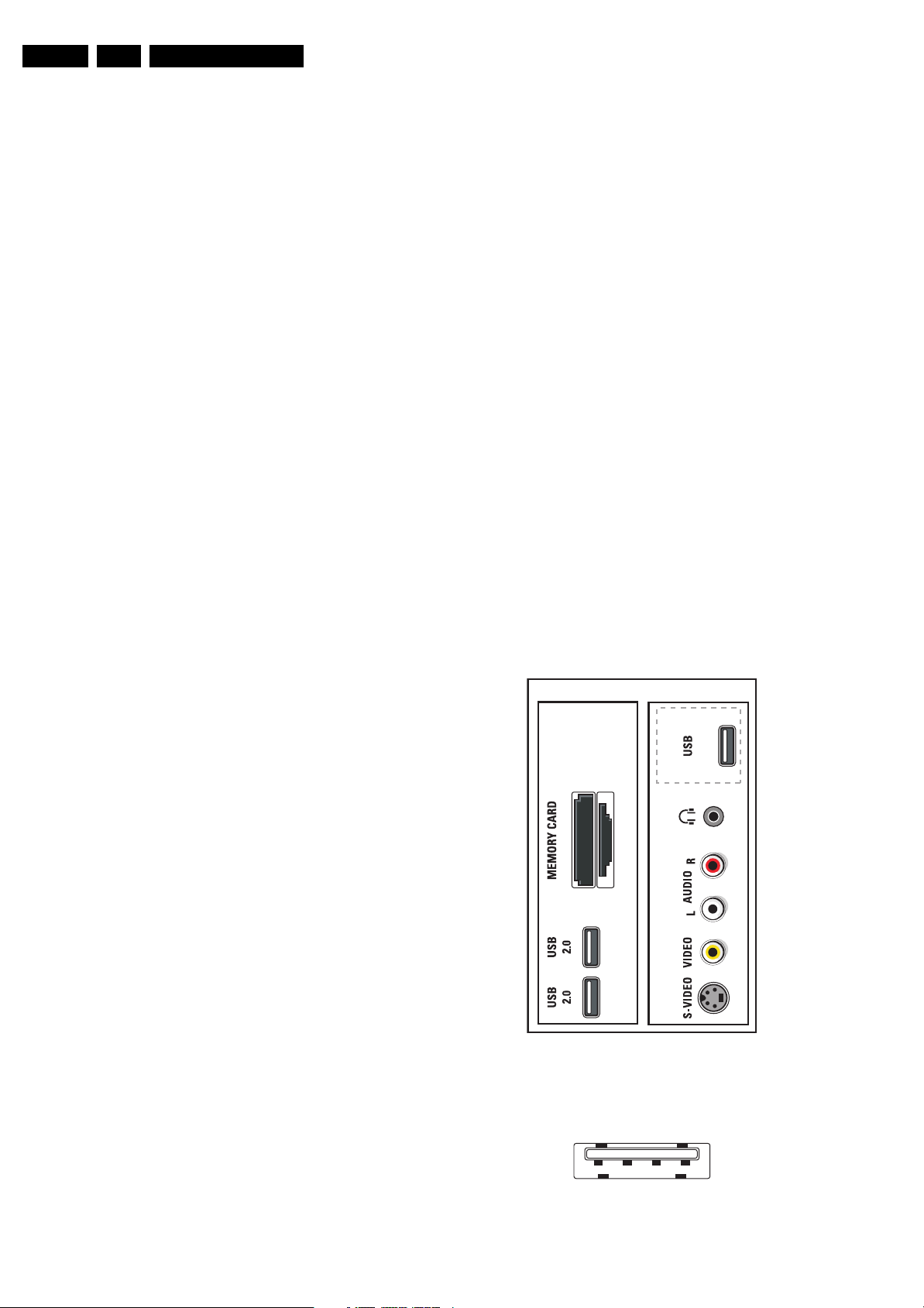
1.2.1 Side Connections
Card reader
For BL/BP2.1, 2.2
Side I/O
For BL/BP2.3
1.1
1.1.2 Sound
Sound systems : AV Stereo
Maximum power (W
1.1.3 Multimedia
Supported digital media : Compact Flash I & II
Supported file formats : JPEG
USB input : USB1.1 (12 Mbps)
) : 2 x 15
RMS
:BTSC
: Memory Stick
: Microdrive (upto 2GB)
: SD / mini SD Card
: Multi Media Card
: Smart Media Card
:MP3
:MP3-pro
: Slideshow (.alb)
USB
E_15570_015.eps
Figure 1-1 Side I/O connections
1234
E_06532_022.eps
Figure 1-2 USB (type A)
130704
300904
Technical Specifications, Connections, and Chassis Overview
EN 3BP2.1U, 2.2U, 2.3U 1.
1-+5V k
2 -Data (-) jk
3 -Data (+) jk
4 -Ground Gnd H
Mini Jack: Audio Headphone - Out
Bk - Headphone 32 - 600 ohm / 10 mW ot
Cinch: Video CVBS - In, Audio - In
Ye - Video CVBS 1 V
Wh - Audio L 0.5 V
Rd - Audio R 0.5 V
/ 75 ohm jq
PP
/ 10 kohm jq
RMS
/ 10 kohm jq
RMS
S-Video (Hosiden): Video Y/C - In
1 -Ground Y Gnd H
2 -Ground C Gnd H
3 - Video Y 1 V
4 - Video C 0.3 V
/ 75 ohm j
PP
P / 75 ohm j
PP
1.2.2 Digital Media Reader with USB2.0 (not for BP2.3)
In some versions, a 6-in-1 card reader unit is available, which
is connected via USB to the Small Signal Board (see also par.
“Technical Specifications” -> “Multimedia”).
This unit also contains two USB2.0 connectors (see figure rear
connections).
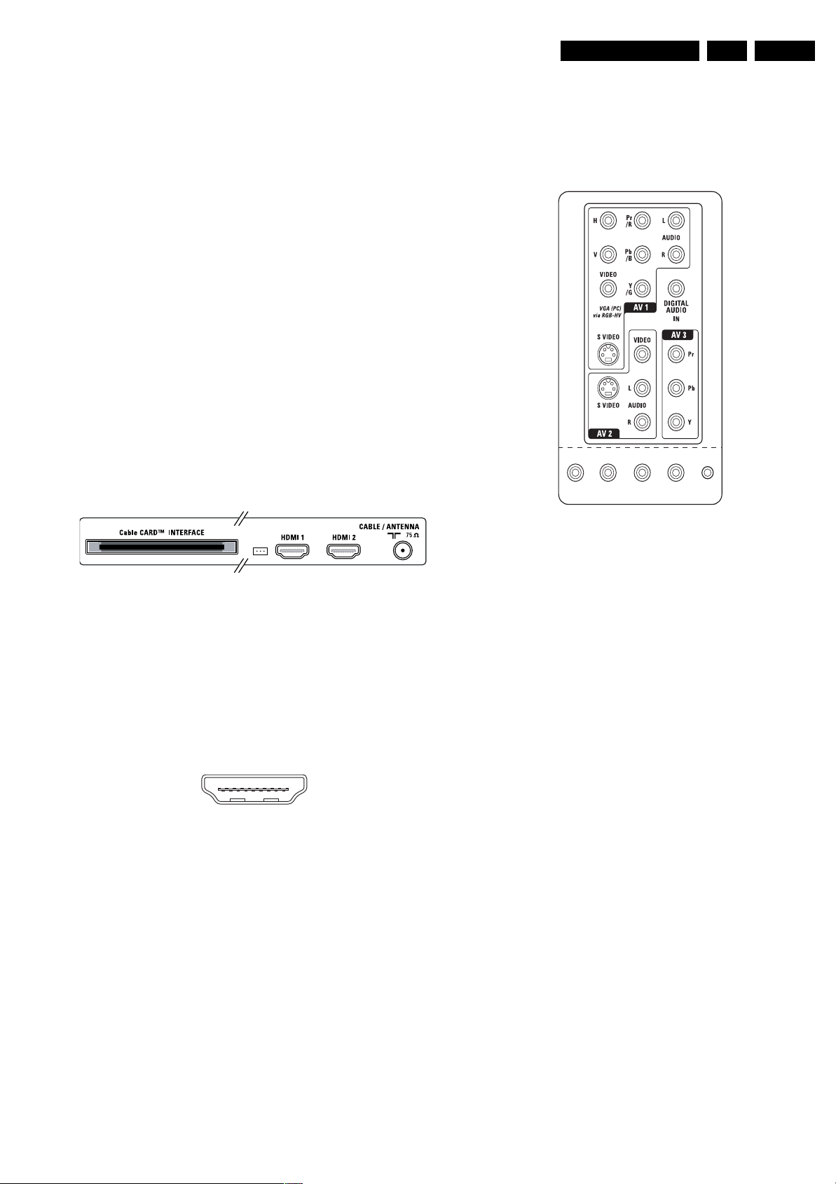
1.2.3 Rear Connections (under side)
20 - Ground Gnd H
Aerial - In
- - F-type (US) Coax, 75 ohm D
1.2.4 Rear Connections (rest)
MONITOR OUT
S/PDIF
L R CVBS GEM
OUT
STAR
F_15400_001.eps
130705
UART
F_15570_009.eps
130705
Figure 1-3 Rear connections (under side)
POD: CableCARD Interface
68p - See diagram B10A jk
Service Connector (UART)
1 - UART_TX Transmit k
2 - Ground Gnd H
3 - UART_RX Receive j
HDMI 1 & 2: Digital Video, Digital Audio - In
19
18 2
1
E_06532_017.eps
250505
Figure 1-4 HDMI (type A) connector
1 - D2+ Data channel j
2 - Shield Gnd H
3 - D2- Data channel j
4 - D1+ Data channel j
5 - Shield Gnd H
6 - D1- Data channel j
7 - D0+ Data channel j
8 - Shield Gnd H
9 - D0- Data channel j
10 - CLK+ Data channel j
11 - Shield Gnd H
12 - CLK- Data channel j
13 - n.c.
14 - n.c.
15 - DDC_SCL DDC clock j
16 - DDC_SDA DDC data jk
17 - Ground Gnd H
18 - +5V j
19 - HPD Hot Plug Detect j
Figure 1-5 Rear connections (rest)
AV1 Cinch: Video YPbPrHV- In
Gn - Video Y 1 V
Bu - Video Pb 0.7 V
Rd - Video Pr 0.7 V
Bk - H-sync 0 - 5 V jq
/ 75 ohm jq
PP
/ 75 ohm jq
PP
/ 75 ohm jq
PP
Bk - V-sync 0 - 5 V jq
AV1 Cinch: Video CVBS - In, Audio - In
Ye - Video CVBS 1 V
Wh - Audio L 0.5 V
Rd - Audio R 0.5 V
/ 75 ohm jq
PP
/ 10 kohm jq
RMS
/ 10 kohm jq
RMS
DIGITAL AUDIO Cinch: S/PDIF - In
Bk - Coaxial 0.2 - 0.6V
/ 75 ohm jq
PP
AV1 S-Video (Hosiden): Video Y/C - In
1 - Ground Y Gnd H
2 - Ground C Gnd H
3 - Video Y 1 V
4 - Video C 0.3 V
/ 75 ohm j
PP
P / 75 ohm j
PP
AV2 S-Video (Hosiden): Video Y/C - In
1 - Ground Y Gnd H
2 - Ground C Gnd H
3 - Video Y 1 V
4 - Video C 0.3 V
/ 75 ohm j
PP
P / 75 ohm j
PP
AV2 Cinch: Video CVBS - In, Audio - In
Ye - Video CVBS 1 V
Wh - Audio L 0.5 V
Rd - Audio R 0.5 V
/ 75 ohm jq
PP
/ 10 kohm jq
RMS
/ 10 kohm jq
RMS
AV3 Cinch: Video YPbPr - In
Rd - Video Pr 0.7 V
Bu - Video Pb 0.7 V
Gn - Video Y 1 V
/ 75 ohm jq
PP
/ 75 ohm jq
PP
/ 75 ohm jq
PP
EN 4 BP2.1U, 2.2U, 2.3U1.
Technical Specifications, Connections, and Chassis Overview
DIGITAL AUDIO Cinch: S/PDIF - Out
Bk - Coaxial 0.4 - 0.6V
/ 75 ohm kq
PP
MONITOR OUT Cinch: Video CVBS - Out, Audio - Out
Ye - Video CVBS 1 V
Wh - Audio L 0.5 V
Rd - Audio R 0.5 V
/ 75 ohm kq
PP
/10 kohm kq
RMS
/ 10 kohm kq
RMS
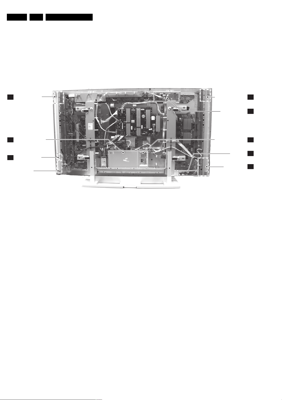
1.3 Chassis Overview
AMBI LIGHT PANEL
AL
(OPTIONAL)
SMALL SIGNAL PANEL
B
CONTROL BOARD
E
GEMSTAR Mini Jack: Remote Control - In/Out
1 - Ground Gnd H
2 - RXD j
3-TXD k
4-IR-OUT k
5 - RXD k
AMBI LIGHT PANEL
(OPTIONAL)
AUDIO AMPLIFIER
EXTERNAL I/O PANEL
LED PANEL
AL
C
BE
J
MULTI MEDIA
CARD READER
(OPTIONAL)
& USB
Figure 1-6 PWB/CBA locations
SIDE I/O PANEL
F_15400_110.eps
D
310505

Safety Instructions, Warnings, and Notes
2. Safety Instructions, Warnings, and Notes
EN 5BP2.1U, 2.2U, 2.3U 2.
Index of this chapter:
2.1 Safety Instructions
2.2 Warnings
2.3 Notes
2.1 Safety Instructions
Safety regulations require that during a repair:
• Connect the set to the Mains/AC Power via an isolation
transformer (> 800 VA).
• Replace safety components, indicated by the symbol h,
only by components identical to the original ones. Any
other component substitution (other than original type) may
increase risk of fire or electrical shock hazard.
Safety regulations require that after a repair, the set must be
returned in its original condition. Pay in particular attention to
the following points:
• Route the wire trees correctly and fix them with the
mounted cable clamps.
• Check the insulation of the Mains/AC Power lead for
external damage.
• Check the strain relief of the Mains/AC Power cord for
proper function.
• Check the electrical DC resistance between the Mains/AC
Power plug and the secondary side (only for sets which
have a Mains/AC Power isolated power supply):
1. Unplug the Mains/AC Power cord and connect a wire
between the two pins of the Mains/AC Power plug.
2. Set the Mains/AC Power switch to the "on" position
(keep the Mains/AC Power cord unplugged!).
3. Measure the resistance value between the pins of the
Mains/AC Power plug and the metal shielding of the
tuner or the aerial connection on the set. The reading
should be between 4.5 Mohm and 12 Mohm.
4. Switch "off" the set, and remove the wire between the
two pins of the Mains/AC Power plug.
• Check the cabinet for defects, to avoid touching of any
inner parts by the customer.
2.2 Warnings
• All ICs and many other semiconductors are susceptible to
electrostatic discharges (ESD w). Careless handling
during repair can reduce life drastically. Make sure that,
during repair, you are connected with the same potential as
the mass of the set by a wristband with resistance. Keep
components and tools also at this same potential. Available
ESD protection equipment:
– Complete kit ESD3 (small tablemat, wristband,
connection box, extension cable and earth cable) 4822
310 10671.
– Wristband tester 4822 344 13999.
• Be careful during measurements in the high voltage
section.
• Never replace modules or other components while the unit
is switched "on".
• When you align the set, use plastic rather than metal tools.
This will prevent any short circuits and the danger of a
circuit becoming unstable.
2.3 Notes
2.3.1 General
• Measure the voltages and waveforms with regard to the
chassis (= tuner) ground (H), or hot ground (I), depending
on the tested area of circuitry. The voltages and waveforms
shown in the diagrams are indicative. Measure them in the
Service Default Mode (see chapter 5) with a color bar
signal and stereo sound (L: 3 kHz, R: 1 kHz unless stated
otherwise) and picture carrier at 475.25 MHz for PAL, or
61.25 MHz for NTSC (channel 3).
• Where necessary, measure the waveforms and voltages
with (D) and without (E) aerial signal. Measure the
voltages in the power supply section both in normal
operation (G) and in stand-by (F). These values are
indicated by means of the appropriate symbols.
• The semiconductors indicated in the circuit diagram and in
the parts lists, are interchangeable per position with the
semiconductors in the unit, irrespective of the type
indication on these semiconductors.
• Manufactured under license from Dolby Laboratories.
“Dolby”, “Pro Logic” and the “double-D symbol”, are
trademarks of Dolby Laboratories.
2.3.2 Schematic Notes
• All resistor values are in ohms and the value multiplier is
often used to indicate the decimal point location (e.g. 2K2
indicates 2.2 kohm).
• Resistor values with no multiplier may be indicated with
either an "E" or an "R" (e.g. 220E or 220R indicates 220
ohm).
• All capacitor values are given in micro-farads (µ= x10
nano-farads (n= x10
• Capacitor values may also use the value multiplier as the
decimal point indication (e.g. 2p2 indicates 2.2 pF).
• An "asterisk" (*) indicates component usage varies. Refer
to the diversity tables for the correct values.
• The correct component values are listed in the Spare Parts
List. Therefore, always check this list when there is any
doubt.
2.3.3 Rework on BGA (Ball Grid Array) ICs
General
Although (LF)BGA assembly yields are very high, there may
still be a requirement for component rework. By rework, we
mean the process of removing the component from the PWB
and replacing it with a new component. If an (LF)BGA is
removed from a PWB, the solder balls of the component are
deformed drastically so the removed (LF)BGA has to be
discarded.
Device Removal
As is the case with any component that, it is essential when
removing an (LF)BGA, the board, tracks, solder lands, or
surrounding components are not damaged. To remove an
(LF)BGA, the board must be uniformly heated to a temperature
close to the reflow soldering temperature. A uniform
temperature reduces the chance of warping the PWB.
To do this, we recommend that the board is heated until it is
certain that all the joints are molten. Then carefully pull the
component off the board with a vacuum nozzle. For the
appropriate temperature profiles, see the IC data sheet.
Area Preparation
When the component has been removed, the vacant IC area
must be cleaned before replacing the (LF)BGA.
Removing an IC often leaves varying amounts of solder on the
mounting lands. This excessive solder can be removed with
either a solder sucker or solder wick. The remaining flux can be
removed with a brush and cleaning agent.
After the board is properly cleaned and inspected, apply flux on
the solder lands and on the connection balls of the (LF)BGA.
Note: Do not apply solder paste, as this has shown to result in
problems during re-soldering.
-9
), or pico-farads (p= x10
-12
-6
),
).
EN 6 BP2.1U, 2.2U, 2.3U2.
Safety Instructions, Warnings, and Notes
Device Replacement
The last step in the repair process is to solder the new
component on the board. Ideally, the (LF)BGA should be
aligned under a microscope or magnifying glass. If this is not
possible, try to align the (LF)BGA with any board markers.
So as not to damage neighboring components, it may be
necessary to reduce some temperatures and times.
More Information
For more information on how to handle BGA devices, visit this
URL: www.atyourservice.ce.philips.com (needs subscription,
not available for all regions). After login, select “Magazine”,
then go to “Workshop Information”. Here you will find
Information on how to deal with BGA-ICs.
2.3.4 Lead Free Solder
Philips CE is producing lead-free sets (PBF) from 1.1.2005
onwards.
Identification: The bottom line of a type plate gives a 14-digit
serial number. Digits 5 and 6 refer to the production year, digits
7 and 8 refer to production week (in example below it is 1991
week 18).
E_06532_024.eps
230205
avoid mixed regimes. If not to avoid, clean carefully the
solder-joint from old tin and re-solder with new tin.
• Use only original spare-parts listed in the Service-Manuals.
Not listed standard material (commodities) has to be
purchased at external companies.
• Special information for lead-free BGA ICs: these ICs will be
delivered in so-called "dry-packaging" to protect the IC
against moisture. This packaging may only be opened
short before it is used (soldered). Otherwise the body of the
IC gets "wet" inside and during the heating time the
structure of the IC will be destroyed due to high (steam)pressure inside the body. If the packaging was opened
before usage, the IC has to be heated up for some hours
(around 90°C) for drying (think of ESD-protection!).
Do not re-use BGAs at all!
• For sets produced before 1.1.2005, containing leaded
soldering tin and components, all needed spare parts will
be available till the end of the service period. For the repair
of such sets nothing changes.
In case of doubt whether the board is lead-free or not (or with
mixed technologies), you can use the following method:
• Always use the highest temperature to solder, when using
SAC305 (see also instructions below).
• De-solder thoroughly (clean solder joints to avoid mix of
two alloys).
Caution: For BGA-ICs, you must use the correct temperatureprofile, which is coupled to the 12NC. For an overview of these
profiles, visit the website www.atyourservice.ce.philips.com
(needs subscription, but is not available for all regions)
You will find this and more technical information within the
"Magazine", chapter "Workshop information".
For additional questions please contact your local repair help
desk.
Figure 2-1 Serial number example
Regardless of the special lead-free logo (which is not always
indicated), one must treat all sets from this date onwards
according to the rules as described below.
P
b
Figure 2-2 Lead-free logo
Due to lead-free technology some rules have to be respected
by the workshop during a repair:
• Use only lead-free soldering tin Philips SAC305 with order
code 0622 149 00106. If lead-free solder paste is required,
please contact the manufacturer of your soldering
equipment. In general, use of solder paste within
workshops should be avoided because paste is not easy to
store and to handle.
• Use only adequate solder tools applicable for lead-free
soldering tin. The solder tool must be able
– To reach at least a solder-tip temperature of 400°C.
– To stabilize the adjusted temperature at the solder-tip.
– To exchange solder-tips for different applications.
• Adjust your solder tool so that a temperature around 360°C
- 380°C is reached and stabilized at the solder joint.
Heating time of the solder-joint should not exceed ~ 4 sec.
Avoid temperatures above 400°C, otherwise wear-out of
tips will rise drastically and flux-fluid will be destroyed. To
avoid wear-out of tips, switch “off” unused equipment or
reduce heat.
• Mix of lead-free soldering tin/parts with leaded soldering
tin/parts is possible but PHILIPS recommends strongly to
2.3.5 Practical Service Precautions
• It makes sense to avoid exposure to electrical shock.
While some sources are expected to have a possible
dangerous impact, others of quite high potential are of
limited current and are sometimes held in less regard.
• Always respect voltages. While some may not be
dangerous in themselves, they can cause unexpected
reactions that are best avoided. Before reaching into a
powered TV set, it is best to test the high voltage insulation.
It is easy to do, and is a good service precaution.
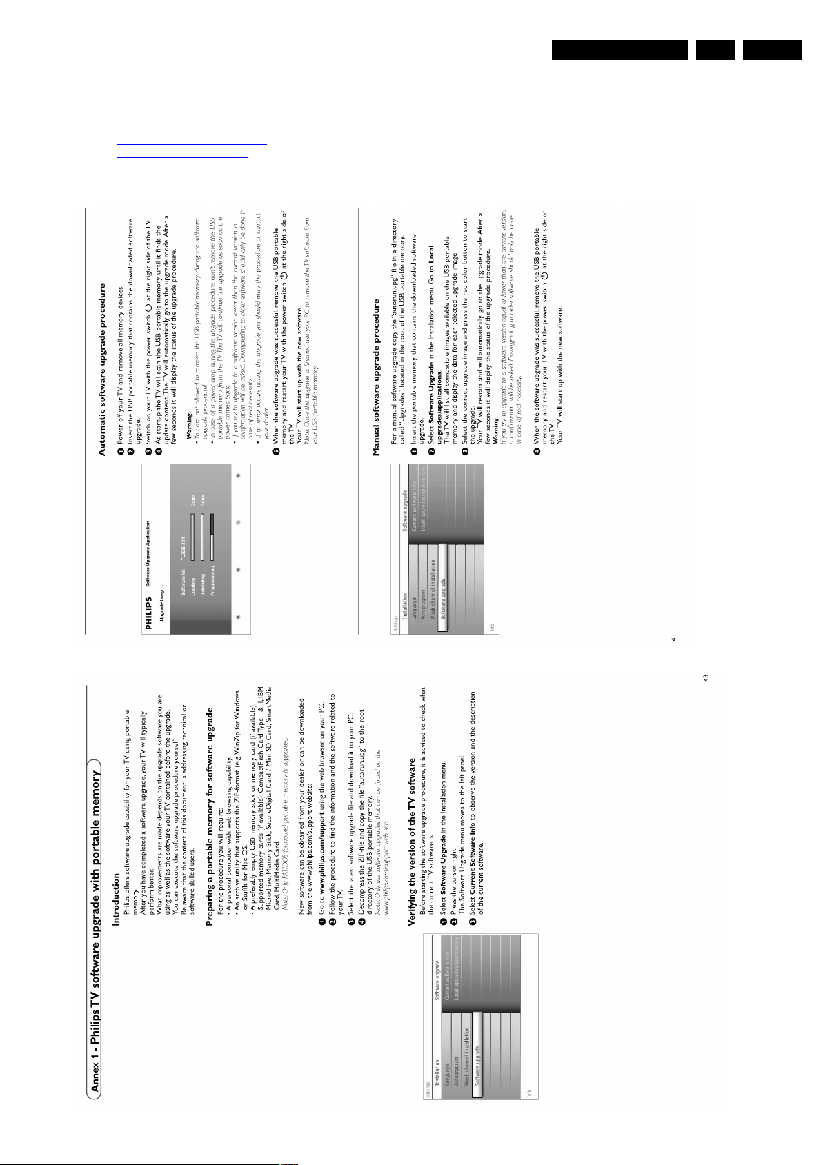
3. Directions for Use
You can download this information from the following websites:
http://www.philips.com/support
http://www.p4c.philips.com
As the software upgrade is a new feature, it is explained below.
Directions for Use
EN 7BP2.1U, 2.2U, 2.3U 3.
EN 8 BP2.1U, 2.2U, 2.3U4.
Mechanical Instructions
4. Mechanical Instructions
Index of this chapter:
4.1 Cable Dressing
4.2 Service Positions
4.3 Assy/Panel Removal
4.4 Set Re-assembly
4.1 Cable Dressing
Notes:
• Figures below can deviate slightly from the actual situation,
due to the different set executions.
• Follow the disassemble instructions in described order.
4.2 Service Positions
For easy servicing of this set, there are a few possibilities
created:
• The buffers from the packaging.
• Foam bars (created for service).
• Aluminium service stands (created for Service).
4.2.1 Foam Bars
E_06532_018.eps
Figure 4-2 Foam bars
The foam bars (order code 3122 785 90580 for two pieces) can
be used for all types and sizes of Flat TVs. By laying the TV
face down on the (ESD protective) foam bars, a stable situation
is created to perform measurements and alignments.
Figure 4-1 Cable dressing (BP2.2U)
By placing a mirror under the TV, you can monitor the screen.
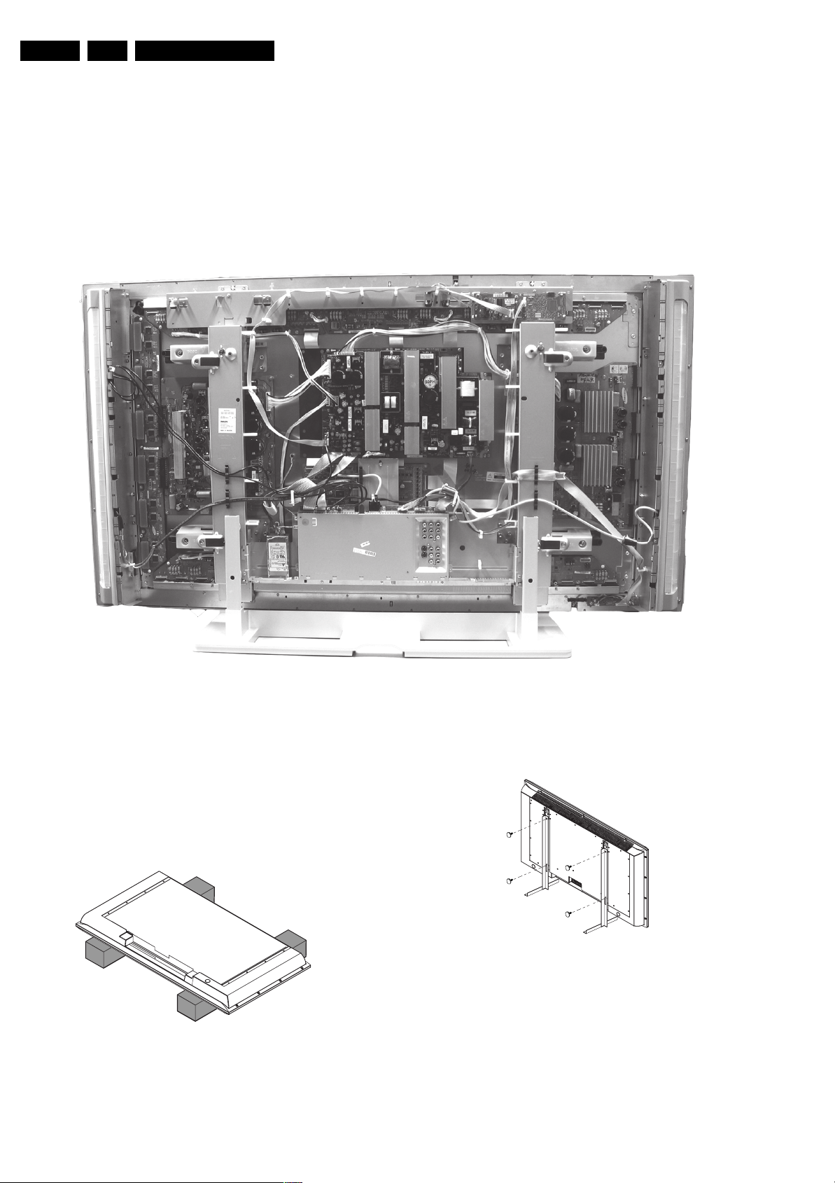
4.2.2 Aluminium Stands
Figure 4-3 Aluminium stands (drawing of MkI)
170504
The new MkII aluminium stands (not on drawing) with order
code 3122 785 90690, can also be used to do measurements,
alignments, and duration tests. The stands can be
(dis)mounted quick and easy by means of sliding them in/out
the "mushrooms". The new stands are backwards compatible
with the earlier models.
Important: For (older) FTV sets without these "mushrooms", it
is obligatory to use the provided screws, otherwise it is possible
to damage the monitor inside!.
F_15400_111.eps
E_06532_019.eps
170504
250505
4.3 Assy/Panel Removal
s
4.3.1 Metal Rear Cover
Caution: Disconnect the Mains/AC Power cord before you
remove the rear cover!
1. Place the TV set upside down on a table top, using the
foam bars (see part "Foam Bars").
Caution: do not put pressure on the display, but let the
monitor lean on the speakers or the Front cover.
2. Remove all T10 screws around the edges of the metal rear
cover: “parker” screws around the outer rim, “tapping”
screws around the connector plate.
3. Remove the four "mushrooms" from the rear cover.
4. Lift the metal rear cover from the set. Make sure that wires
and flat foils are not damaged.
4.3.2 Speaker Compartment Cover
Mechanical Instructions
EN 9BP2.1U, 2.2U, 2.3U 4.
1
After removing the metal rear cover, you gain access to the
Speaker Compartment covers.
1. Remove all T10 screws [1] around the outer rim of the
cover.
2. Remove the T10 screws [2] on top of the inner rim.
3. For sets with AmbiLight: Remove the T10 screws [3] at
the bottom of the inner rim.
4. After removal of all the screws, slightly push the top of the
cover inwards. This will lift the outer rim slightly up so you
can take the cover out.
3
1
3
2
Figure 4-5 AmbiLight inverter panel connections
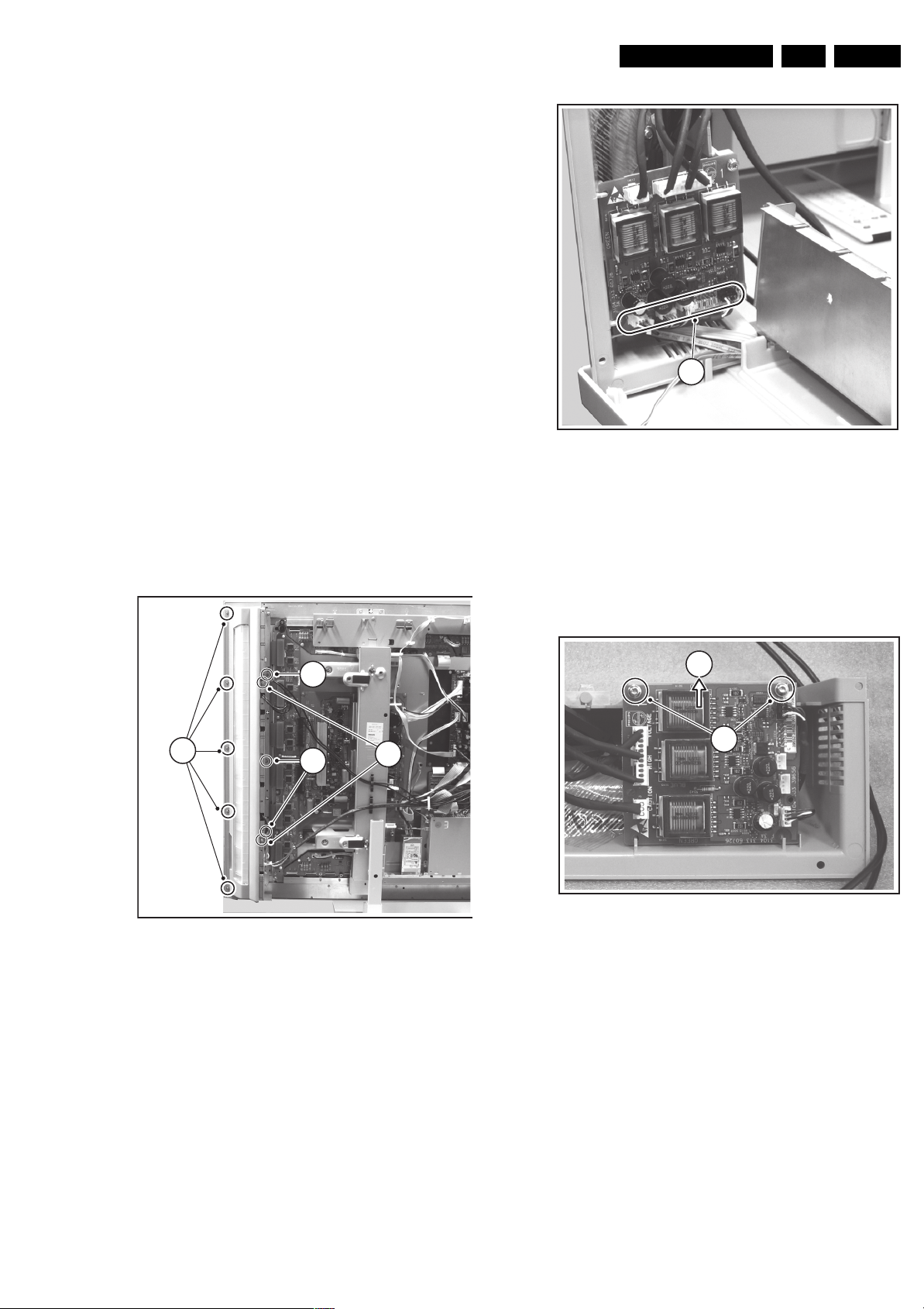
4.3.3 AmbiLight Inverter Panel (if present)
After removal of the Speaker Compartment Covers, this panel
is accessible.
1. Disconnect the cable(s) from the panel.
2. Remove the T10 mounting screws [1] that hold the assy.
3. Take out the panel from its bracket [2].
2
1
F_15400_114.eps
190505
F_15400_112.ep
Figure 4-4 Speaker compartment cover removal
To release the complete cover (only for models with the
AmbiLight feature, as in figure above):
• Lift the cover up; let it hinge at the top side.
• Now, unplug the cables [1] at the AmbiLight Inverter panel.
Figure 4-6 AmbiLight inverter panel removal
4.3.4 Control Panel
After removal of the Speaker Compartment Covers, this panel
is accessible. Release the clamps and take out the panel
4.3.5 Speakers
After removal of the Speaker Compartment Covers, you can
access the speakers.
F_15400_117.eps
190505
EN 10 BP2.1U, 2.2U, 2.3U4.
s
5
Mechanical Instructions
4.3.6 Side I/O Panel
After removal of the Speaker Compartment Covers, this panel
is accessible.
1. Disconnect the cable(s) from the panel.
2. Remove the T10 mounting screws [1] that hold the assy.
3. Take out the panel from its bracket [2].
When defective, replace the whole unit.
2
1
F_15400_116.eps
190505
4.3.9 LED Panel
1. Disconnect the cable(s) from the panel.
2. Remove the T10 mounting screws that hold the panel.
3. Take out the panel.
When defective, replace the whole unit.
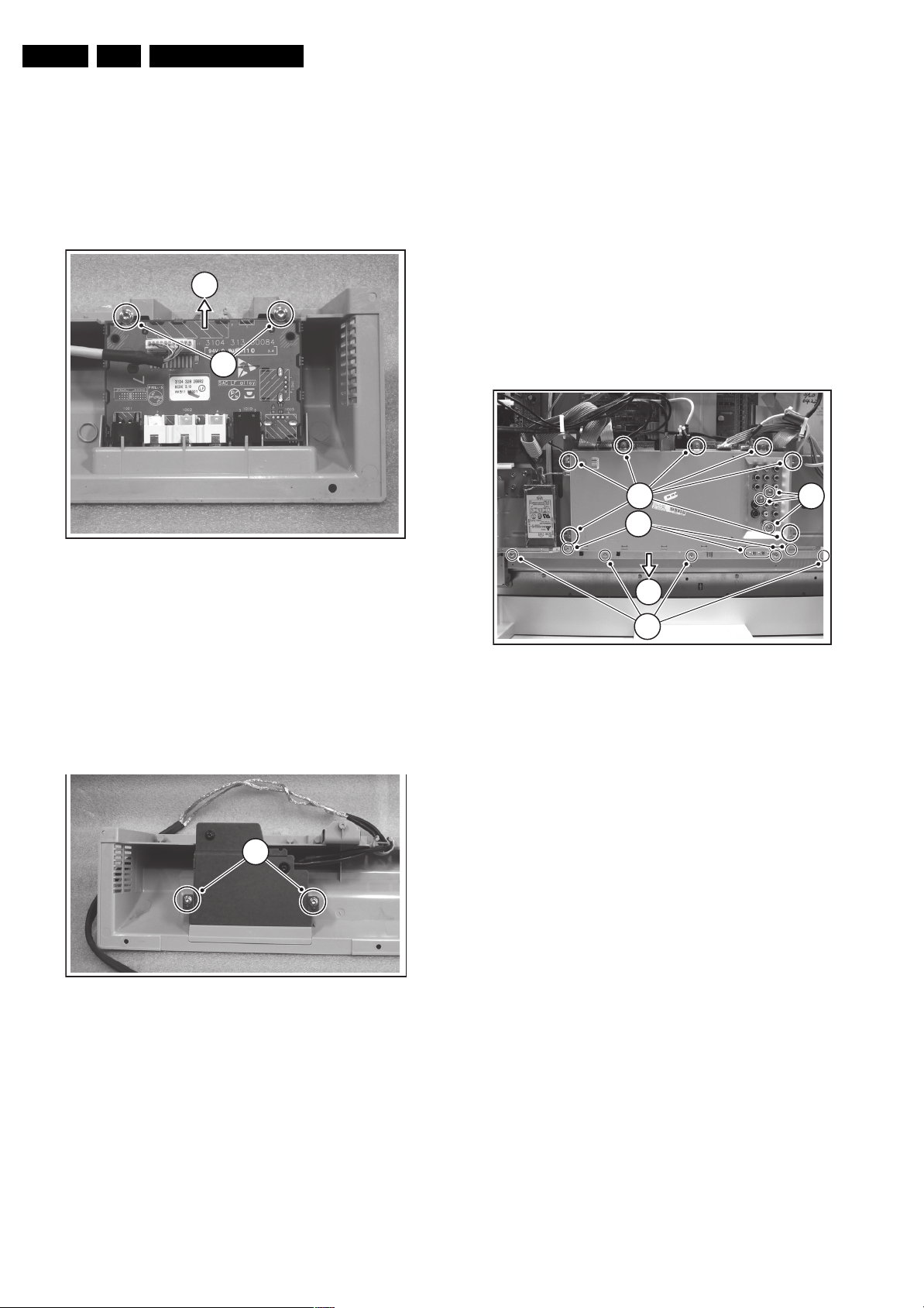
4.3.10 Small Signal Board (SSB)
1. Remove all connector fixation screws [1] at the connector
plate (bottom side), and at the shielding plate (rear side).
2. Remove the fixation screws [2] of the connector plate itself.
3. Remove all shielding fixing screws [3].
4. Slide the connector plate away from the SSB [4], and lift the
shielding from the SSB.
5. Unplug all cables on the SSB.
6. Remove the mounting screws that hold the SSB, and lift
the panel from the set.
3 1
1
Figure 4-7 Side I/O panel removal
4.3.7 Multimedia Card Reader (if present)
After removal of the Speaker Compartment Covers, this panel
is accessible.
1. Unplug the related USB cable at the top of the SSB.
2. Remove the two T10 mounting screws [1] that hold the
assy.
When defective, replace the whole unit.
1
Figure 4-8 Multimedia card reader removal
F_15400_118.ep
19050
4
2
Figure 4-9 SSB top shielding
F_15400_113.eps
190505
4.3.8 Audio Amplifier Panel
1. Disconnect all cables from the Audio Amplifier panel.
2. Remove the T10 mounting screw from the Audio panel.
3. Release the two plastic fixation pins.
4. Take out the Audio panel (it hinges at the top side).
Mechanical Instructions
EN 11BP2.1U, 2.2U, 2.3U 4.
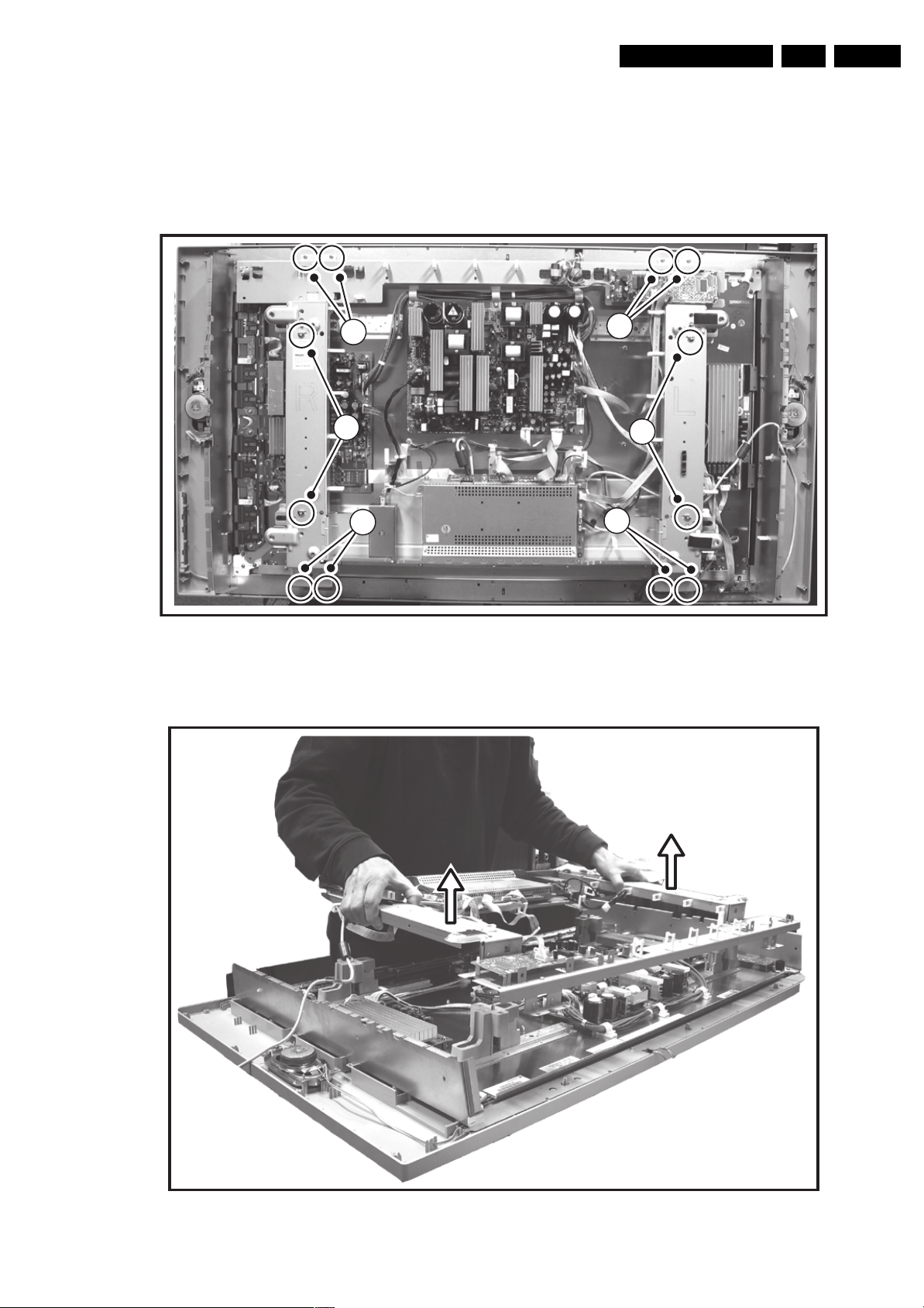
4.3.11 Plasma Display Panel / Glass Plate
1. Remove the T20 display panel mounting screws [1].
2. Remove the T10 screws [2] from the mounting frame.
3. Unplug all cable(s):
– LVDS cable at SSB side (fragile connector!).
– SSB supply cables at the Main Supply board.
– Mains cable at the Main Supply board.
– Side I/O cable at SSB side (fragile connector!).
1
– Cable at LED panel.
– Keyboard cable at SSB side.
– Audio Amplifier supply cable at the Main Supply board.
– Loudspeaker cables (incl. ferrites) at the Audio panel.
4. Lift the metal frame (together with all PWBs) from the
display panel (see figure “Frame lift”).
5. After removal of the frame, lift the PDP from the set.
2
2
1
2
2
Figure 4-10 Display panel removal (photo from LC4.9 chassis)
F_15400_121.eps
200505
Figure 4-11 Frame lift (photo from LC4.9 chassis)
F_15400_120.eps
200505
EN 12 BP2.1U, 2.2U, 2.3U4.
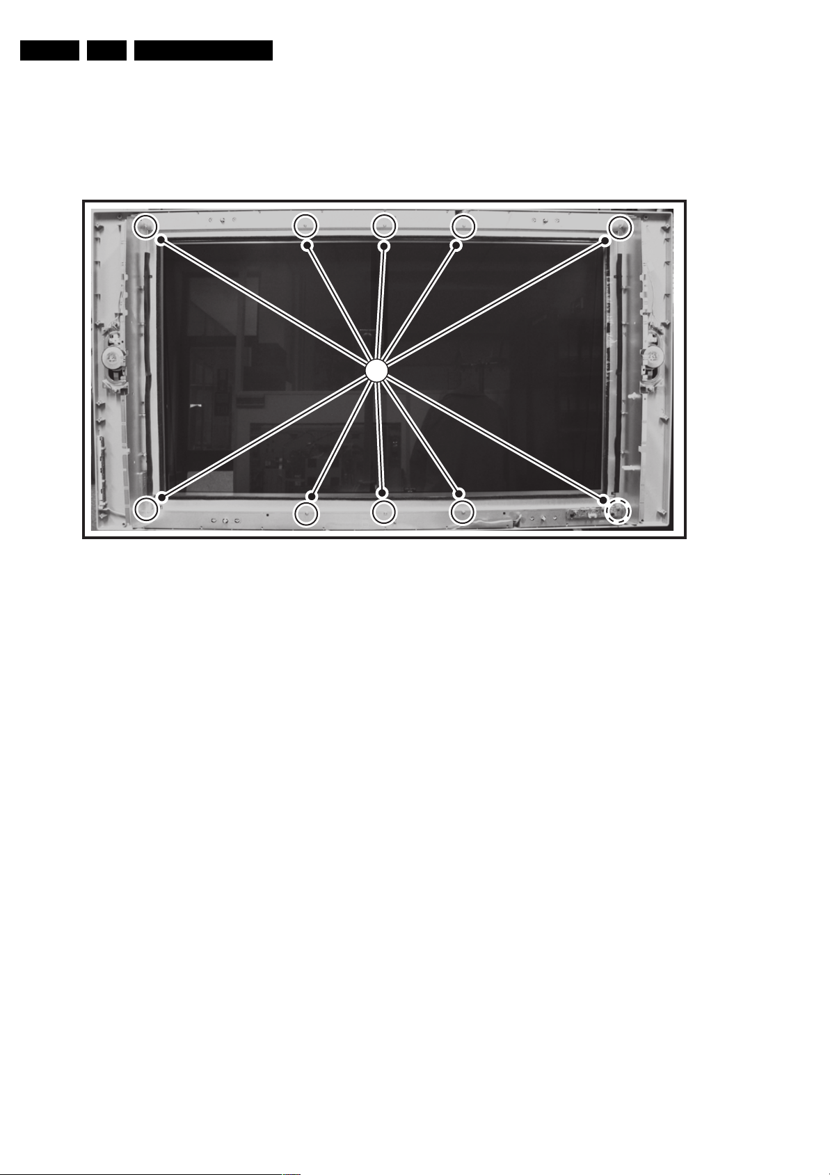
4.3.12 PDP Glass Plate
In order to remove/exchange the PDP glass plate:
1. Remove the PDP as described earlier.
2. Remove the T10 screws [1] from the mounting frame.
3. After removal of the frame, you can lift the glass plate from
the set.
Mechanical Instructions
1
Figure 4-12 Glass plate removal (photo from LC4.9 chassis)
4.4 Set Re-assembly
To re-assemble the whole set, execute all processes in reverse
order.
Notes:
• While re-assembling, make sure that all cables are placed
and connected in their original position. See figure "Cable
dressing".
• Pay special attention not to damage the EMC foams on the
SSB shields. Ensure that EMC foams are mounted
correctly.
F_15400_119.eps
200505
Service Modes, Error Codes, and Fault Finding
5. Service Modes, Error Codes, and Fault Finding
EN 13BP2.1U, 2.2U, 2.3U 5.
Index of this chapter:
5.1 Test Points
5.2 Service Modes
5.3 Stepwise Start-up
5.4 Service Tools
5.5 Error Codes
5.6 The Blinking LED Procedure
5.7 Protections
5.8 Fault Finding and Repair Tips
5.9 Software Upgrading
5.1 Test Points
The chassis is equipped with test points (Fxxx) printed on the
circuit board assemblies. As most signals are digital, it will be
almost impossible to measure waveforms with a standard
oscilloscope. Therefore, waveforms are not given in this
manual. Several key ICs are capable of generating test
patterns, which can be controlled via ComPair. In this way it is
possible to determine which part is defective.
Perform measurements under the following conditions:
• Service Default Mode.
• Video: Color bar signal.
• Audio: 3 kHz left, 1 kHz right.
5.2 Service Modes
Service Default Mode (SDM) and Service Alignment Mode
(SAM) offer several features for the service technician, while
the Customer Service Mode (CSM) is used for communication
between a Customer Helpdesk and a customer.
There is also the option of using ComPair, a hardware interface
between a computer (see requirements below) and the TV
chassis. It offers the ability of structured troubleshooting, test
pattern generation, error code reading, software version
readout, and software upgrading.
Minimum requirements for ComPair: a Pentium processor,
Windows 95/98, and a CD-ROM drive (see also paragraph
“ComPair”).
frequency to which the set will tune, would be as specified
in the channel map and could be different from the one
corresponding to the physical channel 3.
• All picture settings at 50% (brightness, color, contrast).
• All sound settings at 50%, except volume at 25%.
• All service-unfriendly modes (if present) are disabled, like:
– (Sleep) timer.
– Child/parental lock.
– Picture mute (blue mute or black mute).
– Automatic volume levelling (AVL).
– Auto switch "off" (when no video signal was received
for 10 minutes).
– Skip/blank of non-favorite pre-sets.
– Smart modes.
– Auto store of personal presets.
– Auto user menu time-out.
How to Activate SDM
Use one of the following methods:
• Use the standard RC-transmitter and key in the code
“062596”, directly followed by the “MENU” button.
Note: It is possible that, together with the SDM, the main
menu will appear. To switch it "off", push the “MENU”
button again.
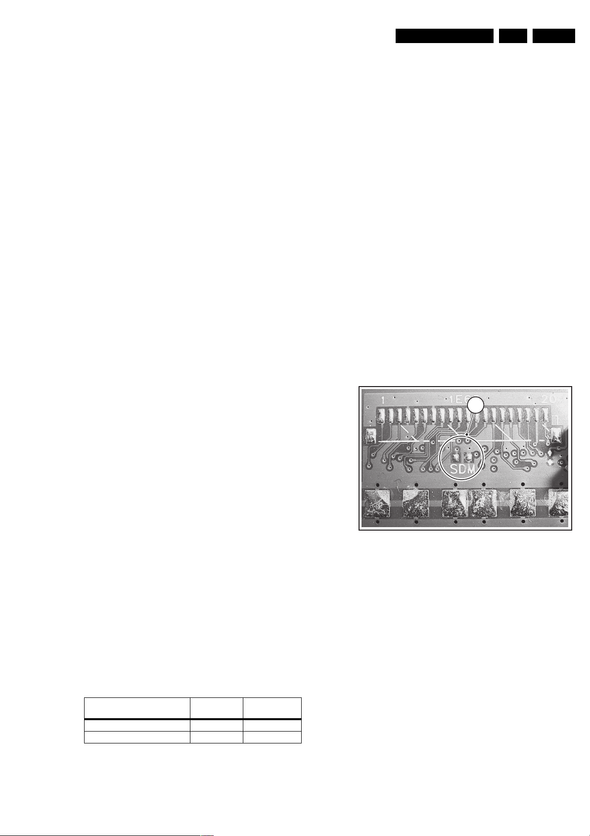
• Short for a moment the two solder pads [1] on the SSB,
with the indication “SDM”. They are located outside the
shielding. Activation can be performed in all modes, except
when the set has a problem with the Stand-by Processor.
See figure “SDM service pads”.
1
5.2.1 Service Default Mode (SDM)
Purpose
• To create a pre-defined setting, to get the same
measurement results as given in this manual.
• To override SW protections (only applicable for protections
detected by stand-by processor) and make the TV start up
to the step just before protection (a sort of automatic
stepwise start up). See paragraph “Stepwise Start Up”.
• To start the blinking LED procedure (not valid in protection
mode).
Specifications
Table 5-1 SDM default settings
Region Freq. (MHz)
Europe, AP-PAL/Multi 475.25 PAL B/G
NAFTA, AP-NTSC, LATAM 61.25 (ch. 3) NTSC M
• Tuning frequency 61.25 MHz for NTSC: The TV shall tune
to physical channel 3 only if channel 3 is an analog channel
or if there is no channel 3 installed in the channel map. If
there is a digital channel installed in channel 3, then the
Default
system
Figure 5-1 SDM service pads
After activating this mode, “SDM” will appear in the upper right
corner of the screen (if you have picture).
How to Navigate
When you press the “MENU” button on the RC transmitter, the
set will toggle between the SDM and the normal user menu
(with the SDM mode still active in the background).
How to Exit SDM
Use one of the following methods:
• Switch the set to STAND-BY via the RC-transmitter.
• Via a standard customer RC-transmitter: key in “00”sequence.
5.2.2 Service Alignment Mode (SAM)
Purpose
• To perform (software) alignments.
• To change option settings.
• To easily identify the used software version.
• To view operation hours.
F_15400_103.eps
110505
EN 14 BP2.1U, 2.2U, 2.3U5.
Service Modes, Error Codes, and Fault Finding
• To display (or clear) the error code buffer.
How to Activate SAM
Via a standard RC transmitter: key in the code “062596”
directly followed by the “INFO” button. After activating SAM
with this method a service warning will appear on the screen,
you can continue by pressing the red button on the RC.
Contents of SAM:
• Hardware Info.
– A. VIPER SW Version. Displays the software version
of the VIPER software (main software) (example:
BX23U-1.2.3.4_12345 = AAAAB_X.Y.W.Z_NNNNN).
• AAAA= the chassis name.
• B= the region: A= AP, E= EU, L= Latam, U = US.
• X.Y.W.Z= the software version, where X is the
main version number (different numbers are not
compatible with one another) and Y is the sub
version number (a higher number is always
compatible with a lower number). The last two
digits are used for development reasons only, so
they will always be zero in official releases.
• NNNNN= last five digits of 12nc code of the
software.
– B. SBY PROC Version. Displays the software version
of the stand-by processor.
– C. Production Code. Displays the production code of
the TV, this is the serial number as printed on the back
of the TV set. Note that if an NVM is replaced or is
initialized after corruption, this production code has to
be re-written to NVM. ComPair will foresee in a
possibility to do this.
• Operation Hours. Displays the accumulated total of
operation hours (not the stand-by hours). Every time the
TV is switched "on/off", 0.5 hours is added to this number.
• Errors. (Followed by maximal 10 errors). The most recent
error is displayed at the upper left (for an error explanation
see paragraph “Error Codes”).
• Defective Module. Here the module that generates the
error is displayed. If there are multiple errors in the buffer,
which are not all generated by a single module, there is
probably another defect. It will then display the message
“UNKNOWN” here.
• Reset Error Buffer. When you press “cursor right” and
then the “OK” button, the error buffer is reset.
• Alignments. This will activate the “ALIGNMENTS” submenu.
• Dealer Options. Extra features for the dealers.
• Options. Extra features for Service.
• Initialise NVM. When an NVM was corrupted (or replaced)
in the former EMG based chassis, the microprocessor
replaces the content with default data (to assure that the
set can operate). However, all preferences and alignment
values are gone now, and option numbers are not correct.
Therefore, this was a very drastic way. In this chassis, the
procedure is implemented in another way: The moment the
processor recognizes a corrupted NVM, the “initialize
NVM” line will be highlighted. Now, you can do two things
(dependent of the service instructions at that moment):
– Save the content of the NVM via ComPair for
development analysis, before initializing. This will give
the Service department an extra possibility for
diagnosis (e.g. when Development asks for this).
– Initialize the NVM (same as in the past, however now it
happens conscious).
Note: When you have a corrupted NVM, or you have replaced
the NVM, there is a high possibility that you will not have picture
any more because your display option is not correct. So, before
you can initialize your NVM via the SAM, you need to have a
picture and therefore you need the correct display option. To
adapt this option, use ComPair. The correct HEX values for the
options can be found in the table below.
Table 5-2 Display option code overview
Display
Option
000 00 PDP SDI HD V3 42” 768p
001 01 PDP SDI HD V3 50” 768p
002 02 PDP FHP ALIS 1024i 42” 1024i
003 03 LPL 30” 768p
004 04 LPL: 37” 768p
005 05 LPL 42” 768p
006 06 SHARP 32” 768p
007 07 PDP SDI SD V3 42” 480p
008 08 PDP FHP ALIS 1024i 37” 1024i
009 09 LCOS XION - 720p
010 0A LCD AUO 30” 768p
011 0B LCD LPL 32” 768p
012 0C LCD AUO 32” 768p
013 0D LCD SHARP 37” 768p
014 0E LCD LPL HD 42” 1080p
015 0F PDP SDI SD 37” 480p
016 10 PDP FHP ALIS 1080i 37” 1080i
017 11 PDP FHP ALIS 580i 42” 1080i
018 12 PDP FHP 55” 768p
019 13 LCOS VENUS - 720p
020 14 LCOS VENUS - 1080p
021 15 LCD LPL 26” 768p
022 16 LCD LPL scanning BL. 32” 768p
023 17 LG SD 42” 480p
024 18 PDP SDI SD V4 42” 480p
025 19 PDP SDI HD V4 42” 768p
026 1A PDP FHP HD A2 42” 1024i
027 1B PDP SDI HD V4 50” 768p
028 1C LCD Sharp full HD 37” 1080p
HEX Display Type Size Vertical
Resolution
• Store. All options and alignments are stored when
pressing “cursor right” and then the “OK”-button
• SW Maintenance.
– SW Events. Not useful for service purposes. In case of
specific software problems, the development
department can ask for this info.
– HW Events. Not functional at the moment this manual
is released, description will be published in an update
manual if the function becomes available.
How to Navigate
• In SAM, you can select the menu items with the “CURSOR
UP/DOWN” key on the RC-transmitter. The selected item
will be highlighted. When not all menu items fit on the
screen, move the “CURSOR UP/DOWN” key to display the
next/previous menu items.
• With the “CURSOR LEFT/RIGHT” keys, it is possible to:
– (De) activate the selected menu item.
– (De) activate the selected submenu.
How to Exit SAM
Use one of the following methods:
• Press the “MENU” button on the RC-transmitter.
• Switch the set to STAND-BY via the RC-transmitter.
Note: As long as SAM is activated, it is not possible to change
a channel. This could hamper the White Point alignments
because you cannot choose your channel/frequency any more.
Workaround: after you have sent the RC code “062596 INFO”
you will see the service-warning screen, and in this stage it is
still possible to change the channel (so before pressing the
“OK” button).

Service Modes, Error Codes, and Fault Finding
EN 15BP2.1U, 2.2U, 2.3U 5.
5.2.3 Customer Service Mode (CSM)
Purpose
When a customer is having problems with his TV-set, he can
call his dealer or the Customer Helpdesk. The service
technician can then ask the customer to activate the CSM, in
order to identify the status of the set. Now, the service
technician can judge the severity of the complaint. In many
cases, he can advise the customer how to solve the problem,
or he can decide if it is necessary to visit the customer.
The CSM is a read only mode; therefore, modifications in this
mode are not possible.
How to Activate CSM
Key in the code “123654” via the standard RC transmitter.
Note: Activation of the CSM is only possible if there is no (user)
menu on the screen!
How to Navigate
By means of the “CURSOR-DOWN/UP” knob on the RCtransmitter, you can navigate through the menus.
Contents of CSM
• SW Version (example: BX23U-1.2.3.4_12345). Displays
the built-in main software version. In case of field problems
related to software, software can be upgraded. As this
software is consumer upgradeable, it will also be published
on the Internet.
• SBY Processor Version. Displays the built-in stand-by
processor software version. Upgrading this software will be
possible via a PC and a ComPair interface (see chapter
Software upgrade).
• Set Type. This information is very helpful for a helpdesk/
workshop as reference for further diagnosis. In this way, it
is not necessary for the customer to look at the rear of the
TV-set. Note that if an NVM is replaced or is initialized after
corruption, this set type has to be re-written to NVM.
ComPair will foresee a possibility to do this.
• Production Code. Displays the production code (the serial
number) of the TV. Note that if an NVM is replaced or is
initialized after corruption, this production code has to be
re-written to NVM. ComPair will foresee a possibility to do
this.
• Code 1. Gives the latest five errors of the error buffer. As
soon as the built-in diagnose software has detected an
error the buffer is adapted. The last occurred error is
displayed on the leftmost position. Each error code is
displayed as a 2-digit number. When less than 10 errors
occur, the rest of the buffer is empty (00). See also
paragraph Error Codes for a description.
• Code 2. Gives the first five errors of the error buffer. See
also paragraph Error Codes for a description.
• Headphone Volume. Gives the last status of the
headphone volume, as set by the customer. The value can
vary from 0 (volume is minimum) to 100 (volume is
maximum). Change via”MENU”, “TV”, “SOUND”,
“HEADPHONE VOLUME”.
• Dolby. Indicates whether the received transmitter
transmits Dolby sound (“ON”) or not (“OFF”). Attention: The
presence of Dolby can only be tested by the software on
the Dolby Signaling bit. If a Dolby transmission is received
without a Dolby Signaling bit, this indicator will show “OFF”
even though a Dolby transmission is received.
• Sound Mode. Indicates the by the customer selected
sound mode (or automatically chosen mode). Possible
values are “STEREO” and “VIRTUAL DOLBY
SURROUND”. Change via “MENU”, “TV”, “SOUND”,
“SOUND MODE”. It can also have been selected
automatically by signaling bits (internal software).
• Tuner Frequency. Not applicable for US sets.
• Digital Processing. Indicates the selected digital mode.
Possible values are “STANDARD” and “PIXEL PLUS”.
Change via “MENU”, “TV”, “PICTURE”, “DIGITAL
PROCESSING”.
• TV System. Gives information about the video system of
the selected transmitter.
– M: NTSC M signal received
– ATSC: ATSC signal received
• Center Mode. Not applicable.
• DNR. Gives the selected DNR setting (Dynamic Noise
Reduction), “OFF”, “MINIMUM”, “MEDIUM”, or
“MAXIMUM”. Change via “MENU”, “TV”, “PICTURE”,
“DNR”
• Noise Figure. Gives the noise ratio for the selected
transmitter. This value can vary from 0 (good signal) to 127
(average signal) and to 255 (bad signal). For some
software versions, the noise figure will only be valid when
“Active Control” is set to “medium” or “maximum” before
activating CSM.
• Source. Indicates which source is used and the video/
audio signal quality of the selected source. (Example:
Tuner, Video/NICAM) Source: “TUNER”, “AV1”, “AV2”,
“AV3”, “HDMI 1”, “SIDE”. Video signal quality: “VIDEO”, “SVIDEO”, “RGB 1FH”, “YPBPR 1FH 480P”, “YPBPR 1FH
576P”, “YPBPR 1FH 1080I”, “YPBPR 2FH 480P”, “YPBPR
2FH 576P”, “YPBPR 2FH 1080I”, “RGB 2FH 480P”, “RGB
2FH 576P” or “RGB 2FH 1080I”. Audio signal quality:
“STEREO”, “SPDIF 1”, “SPDIF 2”, or “SPDIF”.
• Audio System. Gives information about the audible audio
system. Possible values are “Stereo”, ”Mono”, “Mono
selected”, “Analog In: No Dig. Audio”, “Dolby Digital 1+1”,
“Dolby Digital 1/0”, “Dolby Digital 2/0”, “Dolby Digital 2/1”,
“Dolby Digital 2/2”, “Dolby Digital 3/0”, “Dolby Digital 3/1”,
“Dolby Digital 3/2”, “Dolby Digital Dual I”, “Dolby Digital
Dual II”, “MPEG 1+1”, “MPEG 1/0”, “MPEG 2/0”. This is the
same info as you will see when pressing the “INFO” button
in normal user mode (item “signal”). In case of ATSC
receiving there will be no info displayed.
• Tuned Bit. Not applicable for US sets.
• Preset Lock. Indicates if the selected preset has a child
lock: “LOCKED” or “UNLOCKED”. Change via “MENU”,
“TV”, “CHANNELS”, “CHANNEL LOCK”.
• Lock After. Indicates at what time the channel lock is set:
“OFF” or e.g. “18:45” (lock time). Change “MENU”, “TV”,
“CHANNELS”, “LOCK AFTER”.
• TV Ratings Lock. Indicates the “TV ratings lock” as set by
the customer. Change via “MENU”, “TV”, “CHANNELS”,
“TV RATINGS LOCK”. Possible values are: “ALL”,
“NONE”, “TV-Y”, “TV-Y7”, “TV-G”, “TV-PG”, “TV-14” and
“TV-MA”.
• Movie Ratings Lock. Indicates the “Movie ratings lock” as
set by the customer. Change via “MENU”, “TV”,
“CHANNELS”, “MOVIE RATINGS LOCK”. Possible values
are: “ALL”, “NR”, “G”, “PG”, “PG-13”, “R”, “NC-17” and “X”.
• V-Chip Tv Status. Indicates the setting of the V-chip as
applied by the selected TV channel. Same values can be
shown as for “TV RATINGS LOCK”.
• V-Chip Movie Status. Indicates the setting of the V-chip
as applied by the selected TV channel. Same values can
be shown as for “MOVIE RATINGS LOCK”.
• Options 1. Gives the option codes of option group 1 as set
in SAM (Service Alignment Mode).
• Options 2. Gives the option codes of option group 2 as set
in SAM (Service Alignment Mode).
• AVL. Indicates the last status of AVL (Automatic Volume
Level): “ON” or “OFF”. Change via “MENU”, “TV”,
“SOUND”, “AVL”. AVL can not be set in case of digital
audio reception (e.g. Dolby Digital or AC3)
• Delta Volume. Indicates the last status of the delta volume
for the selected preset as set by the customer: from “-12”
to “+12”. Change via “MENU”, “TV”, “SOUND”, “DELTA
VOLUME”.
• HDMI key validity. Indicates the key’s validity.
• IEEE key validity. Indicates the key’s validity (n.a.).
• POD key validity. Indicates the key’s validity.
• Digital Signal Quality. Indicates quality of the received
digital signal (0= low).
EN 16 BP2.1U, 2.2U, 2.3U5.
How to Exit CSM
Press any key on the RC-transmitter (with exception of the
“CHANNEL +/-”, “VOLUME”, “MUTE” and digit (0-9) keys).
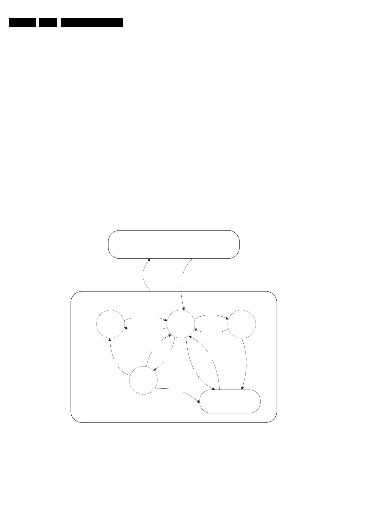
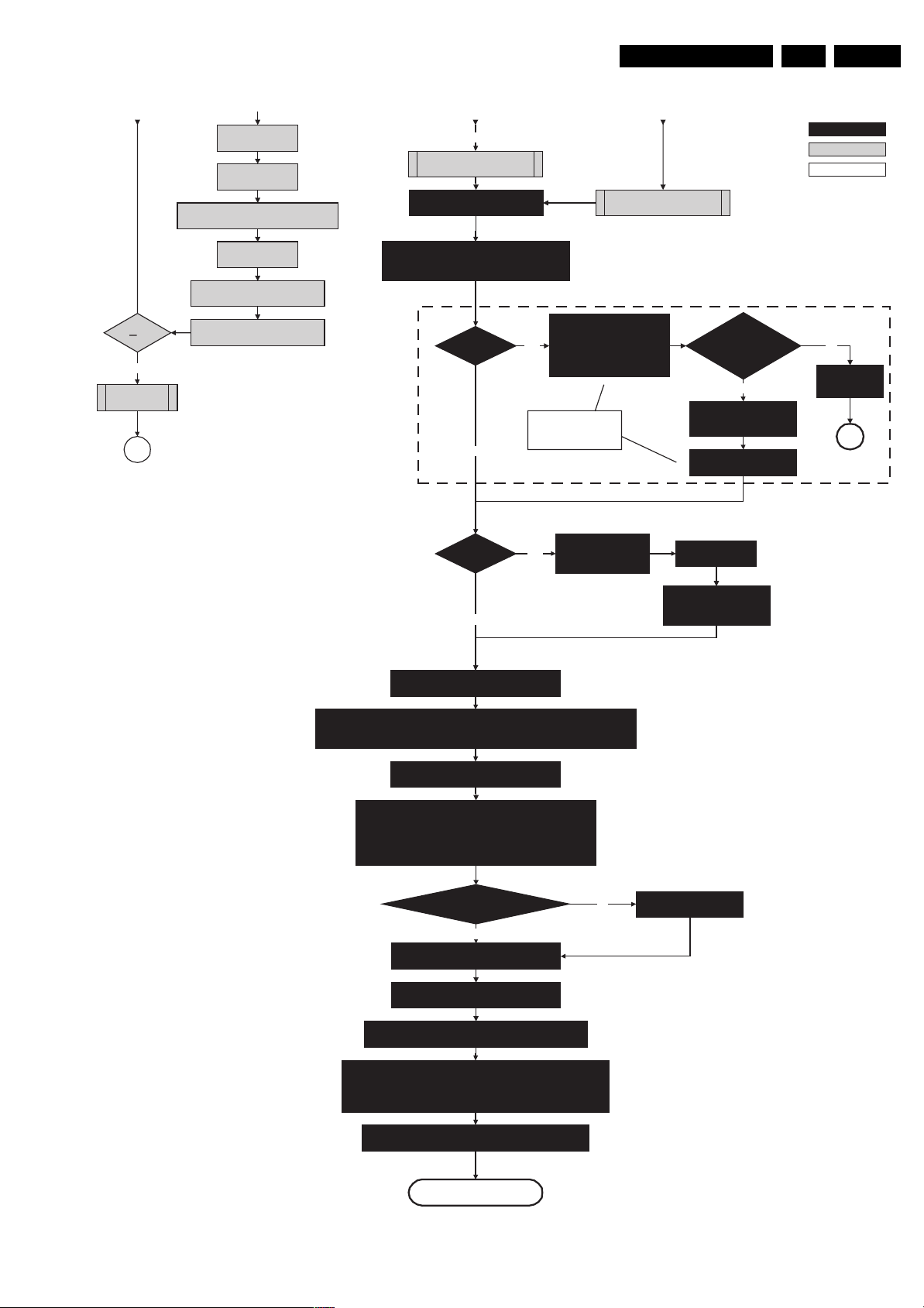
5.3 Stepwise Start-up
The stepwise start-up method, as known from FTL/FTP sets is
not valid any more. The situation for this chassis is as follows:
when the TV is in a protection state detected via the Stand-by
Processor (and thus blinking an error) and SDM is activated via
shortcutting the pins on the SSB, the TV starts up until it
reaches the situation just before protection. So, this is a kind of
automatic stepwise start-up. In combination with the start-up
diagrams below, you can see which supplies are present at a
certain moment.
Important to know here is, that if e.g. the 3V3 detection fails
(and thus error 11 is blinking) and the TV is restarted via SDM,
the Stand-by Processor will enable the 3V3, but will not go to
protection now. The TV will stay in this situation until it is reset
(Mains/AC Power supply interrupted).
The abbreviations “SP” and “MP” in the figures stand for:
• SP: protection or error detected by the Stand-by
Processor.
• MP: protection or error detected by the VIPER Main
Processor.
Service Modes, Error Codes, and Fault Finding
On
Stand-by
(Off St-by)
- POD Card remove
- Tact SW pushed
Mains
“off”
- WakeUp requested
- Acquisition needed
- No data Acquisition required
and no POD present
- Tact SW pushed
- WakeUp requested
- Acquisition needed
d
POD
Stand-by
Off
Semi
Stand-by
No data Acquisition
required and
POD present
GoToProtection
Mains
“on”
GoToProtection
WakeUp
requested
- St-by requested
- Tact SW pushed
WakeUp
requested
Protection
Active
GoToProtection
F_15400_095.eps
300505
Figure 5-2 Transition diagram
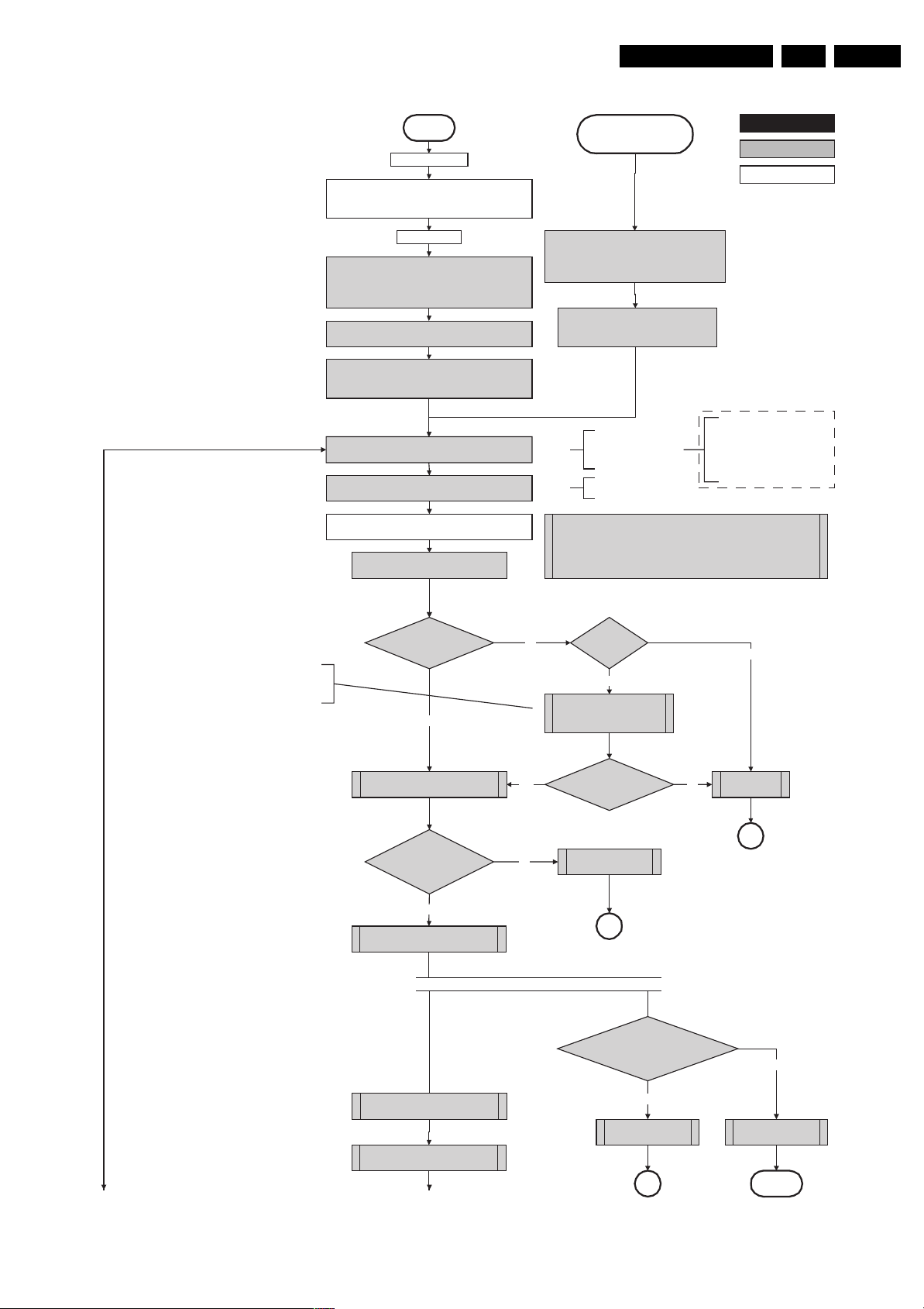
Service Modes, Error Codes, and Fault Finding
EN 17BP2.1U, 2.2U, 2.3U 5.
Off
Mains is applied
Standby Supply starts running.
+5V2, 1V2Stb, 3V3Stb and +2V5D become present.
In case of PDP 3V3 Vpr to CPU PDP becomes present.
st-by µP resets
All I/O lines have a “high” default state:
- Sound-Enable and Reset-Audio should remain “high”.
- NVM power line is “high”, no NVM communication possible.
Initialise I/O pins of the st-by µP, start keyboard scanning, RC
CPUGO (inverse of the stby I/O line POD-MODE) and PDPGO
are then both “low” and the PDP is in the “low power” mode.
Switch “low” the NVM power reset line. Add a 2ms delay
before trying to address the NVM to allow correct NVM
Switch “on” all supplies by switching LOW the POD-MODE
+5V, +8V6, +12VS, +12VSW and Vsound are switched on
- Assert the Viper reset.
detection, P50 decoding. Wake up reasons are “off”.
In case of FHP PDP: Switch PDPGO “low”
initialization.
and the ON-MODE I/O lines.
Wait 50ms and then sta rt polling the detect-
5V, detect-8V6 and detect-12V every 40ms.
Stand-by or
Protection
action holder: MIPS
action holder: St-by
autonomous action
If the protection state was left by short circuiting the
SDM pins, detection of a protection condition during
startup will stall the startup. Protection conditions in a
playing set will be ignored. The protection mode will
- Switch Sound-Enable and Reset-Audio “high”.
The availa bility of the supplies is ch ecked through detect signals (deliv ered by
dedicated detect-IC's) going to the st-by µP. These signals are available for
+12V, +8V6, +5V, +1V2 and +2V5. A low to high transition of the signals should
occur within a certain time after toggling the standby line. If an observers is
detected before the time-out elapses, of course, the process should continue in
not be entered.
They are “low” in the standby mode if the
standby mode lasted longer than 2s.
Switching the POD-MODE
low in an FHP PDP set
makes the CPUGO go “high”
and starts the PDP CPU.
except i n an FHP PDP Cold
Boot
order to minimize start up time.
Switching the POD-MODE and the
“on” mode “low” in an SDI PDP se t
makes the PDP supplies go to the
“on” mode. Within 4 seconds, a
valid LVDS must be sen t to the
display to prev ent protection.
(valid for V3 version)
Switching the PDPGO “high”
will give a visual arte fact and
should only be done if really
necessary.
detect-5V
received within
2900 ms after POD-MODE
toggle?
Yes
activate +5V supply detection algorithm
detect-12VSW received within
2900 ms after POD-mode
toggle?
Yes
activate +12VSW supply
detection algorithm
No need to wait for the 8V6 detection at this point.
No
PDP should start: 5V, 8V6 and
Yes
No
FHP PDP Set?
Yes
Switch PDPGO hig h:
12V are activated
detect-5V
received within
2900 ms after PDPGO
toggle?
+12V error
SP
detect-8V6 received
within 6300 ms after POD-mode toggle?
Startup shall not wait for this detection
and continue startup.
No
+5V error
No
SP
Yes
Enable the +1V2 supply (ENABLE-1V2)
Start polling the detect-1V2 every 40ms
To part B To part B
Figure 5-3 “Off” to “Semi Stand-by” flowchart (part 1)
No
+8V6 erro r
SP
activate +8V6 supply
detection algorithm
return
F_15400_096a.eps
100505
EN 18 BP2.1U, 2.2U, 2.3U5.
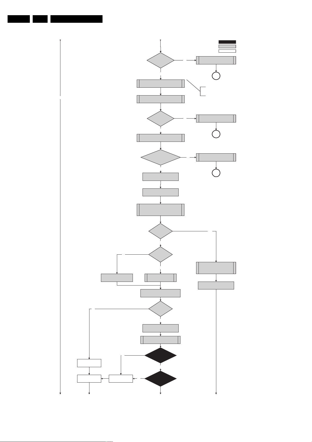
Service Modes, Error Codes, and Fault Finding
From part A
No
From part B
detect-1V2
received within
250ms?
Yes
Enable the supply for
+2.5V and +3.3V (ENABLE-3V3)
Start polling the detect-3V3 every 40ms
detect-3V3
received within
250 ms?
Yes
Activate supply detection algorithms for
+1V2 and +3V3
SUPPLY-FAULT I/O line
is High?
Yes
Enable the supply fault detection
interrup t
action holder: MIPS
action holder: St-by
autonomous action
No
+1.2V error
SP
No separate enable and
detect is present for the +2V5
supply in the Baby Jaguar.
+3.3V errorNo
SP
Supply fault errorNo
SP
No
No
Release viper reset
Feed warm boot script(2)
Set I²C slave address
of Standby µP to (A0h)
Detect EJTAG debug probe
(pulling pin of the probe interface to
ground by inserting EJTAG probe)
EJTAG pro be
connected ?
No
Cold boot?
Yes
Release viper reset
Feed cold boot script(1)
Release PNX2015 reset 100ms after
Viper reset is released
Bootscript ready
in 1250 ms?
Yes
Set I²C slave address
of Standby µP to (64h)
RPC start (comm. protocol)
Yes
Release viper reset
Feed initializing boot script (3)
disable alive mechanism
Release PNX2015 reset 100ms
after Viper reset is released
No
Flash to RAM image
transfer succeeded
within 30s?
Yes
Viper SW initialization
succeeded
within 20s?
Code = 5
Switch Viper in reset
No
Code = 53
To part C To part C To part C To part C
F_15400_096b.eps
Figure 5-4 “Off” to “Semi Stand-by” flowchart (part 2)
260505
Service Modes, Error Codes, and Fault Finding
EN 19BP2.1U, 2.2U, 2.3U 5.
From part B From part B From part B
Yes
Enable Alive check mechanism
from standby µP.
SDI PDP
Set?
No
FHP PDP
Set?
Switch “on” the LVDS output of
the PNX2015 with a correct
clock frequency within 4s after
Yes
switching the POD and “on”
mode to prevent PDP display
supply protection.
These LVDS items are
SDI V3 displ ay only ! !
Yes
Send ST BYEN = 1
to PDP displ ay (I²C)
PFCON = 1
VCCON = 1
Wait until Viper starts to
communicate
3-th try?
Yes
Log Code as
error code
SP
Wait 10ms
Switch the NVM reset
line HIGH.
Disable all supply related protections and
switch off the +2V5, +3V3 DC/DC converter.
Wait 5ms
switch off the remaining DC/DC
converters
Switch POD- MODE a nd ON-MODE
I/O line “high”.
MIPS reads the wake up reason
Wait for the +8V6 to be detected if not yet present. (if
it does not come, the standby µP will enter a
protection mode, this is not a dead end here)
PWR-OK- PDP
received within 10s
after POD and “on” mode
toggle ?
Yes
Init SDI PDP
Switch LVDS back off if
end state is not the active
state.
Switch PDPGO “ low”
action holder: MIPS
action holder: St-by
autonomous action
No
Log display
error and enter
protection mode
SP
No
Start 4 seconds preheating timer in case of
a LPL scanning backlight LCD set.
AVIP needs to be started before the MPIF in order to have a good clock distribution.
AVIP default power-up mode is Standby. The Viper instructs AVIP via I²C to enable all the
PLLs and clocks and hence enter to Full Power mode.
Initialize PNX2015 HD subsystem
MPIFs should be initialized
MPIF should deliver 4 observers:
POR= 0; normal operation
MSUP = 1: Main supply is present
ASUP = 1; audio supply is present
ROK = 1; reference frequency is present (coming from AVIP)
All observers present with correct state?
Yes
Initialize tuners and HDMI
Initialize source select ion
Initialize video processing ICs
- Spider (if available)
No
Init FHP PDP
Log appropriate
Observer error
Initialize Columbus
Initialize 3D Combfilt er
Initialize AutoTV
Do not enter semi-standby state in case of an LPL
scanning backlight LCD set before 4 s preheating timer has
elapsed.
Semi-Stand-by
Figure 5-5 “Off” to “Semi Stand-by” flowchart (part 3)
F_15400_096c.eps
260505
EN 20 BP2.1U, 2.2U, 2.3U5.
Service Modes, Error Codes, and Fault Finding
42" / 50" SDI V4
Semi Stand-by
action holder: MIPS
action holder: St-by
RGB video blanking
and audio mute.
Initialize audio and video processing ICs and
functions.
Wait untill QVCP generates a valid LVDS
output clock
Switch “on” LVDS transmitter
(PNX2015) (if not already on).
Switch the SDI Picture Flag “low” to enable picture. 1.5
seconds later, the display will unblank automatically
and show the LVDS content.
Enable anti-aging
(if applicable).
autonomous action
Switch “off” RGB blanking after valid, stable video.
Switch Audio-Reset and sound enable “low” and demute.
Active
Figure 5-6 “Semi Stand-by” to “Active” flowchart
F_15400_097.eps
260505
Service Modes, Error Codes, and Fault Finding
42" / 50" SDI V4
EN 21BP2.1U, 2.2U, 2.3U 5.
Active
Mute all sound outputs.
Switch RESET_AUDIO and
SOUND_ENABLE lines “high”
Blank PDP display.
Mute all video outputs.
Wait 600ms to prevent image
retention
(display error)
action holder: MIPS
action holder: St-by
autonomous action
Switch “off” LVDS signal
(PNX2015).
Switch the SDI Picture Flag “high” to prevent
testpattern display in semi-standby mode
Semi Stand-by
Figure 5-7 “Active” to “Semi Stand-by” flowchart
F_15400_098.eps
260505
EN 22 BP2.1U, 2.2U, 2.3U5.
Service Modes, Error Codes, and Fault Finding
POD
Transfer Wake up reasons to the
Stand- by µP.
Images are re-transferred to DDR-RAM from
Flash RAM (verification through checksum).
MIPS image completes the application reload,
stops DDR-RAM access, puts itself in a
sleepmode, and signals the standby µP when
the Stand-by mode can be entered.
DDR-RAM is put in self refresh mode and the images
are kept in the hibernating DDR-RAM.
Wait 5ms
Semi Stand-by
action holder: MIPS
action holder: St-by
autonomous action
Important remark:
release RESET AUDIO and
SOUND_ENABLE 2 sec after
entering stand-by to save power
Switch Viper in reset state
Wait 10ms
Switch the NVM reset line “high”.
Disable all supply related protections and switch “off”
the +2V5, +3V3 DC/DC converter.
Wait 5ms
Switch “off” the remaining DC/DC converters
Switch “off” all supplies by switching “high” the POD-
MODE and the ON-MODE I/O lines.
For PDP this means
CPUGO becomes low.
Stand-by
Figure 5-8 “Semi Stand-by” / ”POD” to “Stand-by” flowchart
F_15400_099.eps
260505
Service Modes, Error Codes, and Fault Finding
EN 23BP2.1U, 2.2U, 2.3U 5.
action holder: MIPS
action holder: St-by
autonomous action
Power-down HDMI and 1394 hardware by keeping
Set Viper HW blocks (TM1, TM2, MBS, VMSP1 and
Semi Stand-by
This state transition is entered when stand-by is
requested and an authenticated POD is present.
Reboot
POWERDOWN-1394-GPIO- 0 line “high”.
VMSP2) to powerdown mode.
Hibernate the PNX2015 memory and keep the
PNX2015 in reset state
Disable +8V6 supply detection algorithm
Disable audio protection algorithm
Switch “off” all supplies which are not needed in POD
standby by switching “high” the ON-MODE I/O line.
POD Stand-by
Figure 5-9 “Semi Stand-by” to “POD Stand-by” flowchart
F_15400_100.eps
260505

EN 24 BP2.1U, 2.2U, 2.3U5.
Service Modes, Error Codes, and Fault Finding
POD stand by
action holder: MIPS
action holder: St-by
autonomous action
Switch “on” all supplies by switching “low”
the ON-MODE I/O line.
Full SSB power and the display related supplies
become available
+8V6
detected within
200 ms after ON-MODE
toggle?
Yes
activate +8V6 supply
detection algorithm
Wait 2000ms to allow main supply to
deliver full power.
Enable audio protection algorithm
SDI PDP
Set?
No
Yes
These LVDS items are
SDI V3 display only !!
No
Switch “on” the LVDS output
the PNX2015 with a correct
clock frequency within 4s after
switching the POD and ON-
mode to prevent PDP display
supply protection.
+8V6 error
SP
PWR-OK-PDP
received within 5s after
POD and ONmode
toggle ?
Yes
Init SDI PDP
Switch LVDS back “off” if end
state is not the active state.
No
Log display error
and enter
protection mode
SP
Power-up HDMI and 1394 hardware by putting
POWERDOWN-1394 GPIO 0 line “low”.
Enable Viper HW blocks (T M1, TM2, MBS, VMSP1 and
VMSP2) which were in powerdown mode.
Release PNX2015 reset
(AVIPs must be started before the MPIFs in order to have a good clock distribution).
AVIP default power-up mode is Stand-by. The Viper instructs AVIP via I2C to enable all the
PLLs and clocks and hence enter to Full Power mode.
initialize PNX2015 HD subsystem
Initialize MPIFs
MPIF should deliver 4 observers:
POR= 0; normal operation
MSUP = 1: Main supply is present
ASUP = 1; audio supply is present
ROK = 1; reference frequency is present (coming from AVIP)
All observers present with correct state?
Yes
Initialize tuners and Hirate
Initialize source selection
No
appropriate Observer error
MP
Initialize video processing ICs
- Spider (if available)
Initialize Columbus
Initialize 3D Combfilter
Initialize AutoTV
Semi-Stand-by
Figure 5-10 “POD Stand-by” to “Semi Stand-by” flowchart
F_15400_101.eps
120505
Service Modes, Error Codes, and Fault Finding
EN 25BP2.1U, 2.2U, 2.3U 5.
action holder: MIPS
action holder: St-by
autonomous action
If needed to speed up this transition,
this block could be omitted. This is
depending on the outcome of the
safety investigations.
min. 0.5ms to max. 50ms after LVDS switch “off”. (for LCD sets)
MP
Log the appropriate error and
set stand-by flag in NVM
Redefine wake up reasons for protection
state and transfer to stand-by µP.
Switch “off” LCD lamp supply (for LCD sets)
Wait 250ms (min. = 200ms)
Switch “off” LVDS signal
Switch “off” 12V LCD supply within a time frame of
Ask stand-by µP to enter protection state
SP
Switch Viper in reset state
Wait 10ms
Switch the NVM reset line “high”.
Disable all supply related protections and switch “off”
the +2V5, +3V3 DC/DC converter.
Wait 5ms
Switch “off” the remaining DC/DC converters
Switch “off” all supplies by switching “high” the POD-
MODE and the ON-MODE I/O lines.
Flash LED in order to indicate
protection state*.
(*): This can be the standby LED or the ON LED
depending on the availability in the set under
Protection
discussion.
F_15400_102.eps
120505
Figure 5-11 “Protection” flowchart

EN 26 BP2.1U, 2.2U, 2.3U5.
5.4 Service Tools
5.4.1 ComPair
Introduction
ComPair (Computer Aided Repair) is a service tool for Philips
Consumer Electronics products. ComPair is a further
development on the European DST (service remote control),
which allows faster and more accurate diagnostics. ComPair
has three big advantages:
1. ComPair helps you to quickly get an understanding on how
to repair the chassis in a short time by guiding you
systematically through the repair procedures.
2. ComPair allows very detailed diagnostics (on I
is therefore capable of accurately indicating problem areas.
You do not have to know anything about I
yourself because ComPair takes care of this.
3. ComPair speeds up the repair time since it can
automatically communicate with the chassis (when the
microprocessor is working) and all repair information is
directly available. When ComPair is installed together with
the Force/SearchMan electronic manual of the defective
chassis, schematics and PWBs are only a mouse click
away.
Specifications
ComPair consists of a Windows based fault finding program
and an interface box between PC and the (defective) product.
The ComPair interface box is connected to the PC via a serial
(or RS-232) cable.
For this chassis, the ComPair interface box and the TV
communicate via a bi-directional service cable via the service
connector(s).
The ComPair fault finding program is able to determine the
problem of the defective television. ComPair can gather
diagnostic information in two ways:
• Automatically (by communicating with the television):
ComPair can automatically read out the contents of the
entire error buffer. Diagnosis is done on I
ComPair can access the I
ComPair can send and receive I
the microcontroller of the television. In this way, it is
possible for ComPair to communicate (read and write) to
devices on the I
2
C/UART buses of the TV-set.
• Manually (by asking questions to you): Automatic
diagnosis is only possible if the microcontroller of the
television is working correctly and only to a certain extent.
When this is not the case, ComPair will guide you through
the fault finding tree by asking you questions (e.g. Does the
screen give a picture? Click on the correct answer: YES /
NO) and showing you examples (e.g. Measure test-point I7
and click on the correct oscillogram you see on the
oscilloscope). You can answer by clicking on a link (e.g.
text or a waveform picture) that will bring you to the next
step in the fault finding process.
By a combination of automatic diagnostics and an interactive
question / answer procedure, ComPair will enable you to find
most problems in a fast and effective way.
2
C/UART bus of the television.
2
C/UART commands to
Service Modes, Error Codes, and Fault Finding
2
C level) and
2
C commands
2
C/UART level.
5.4.2 LVDS Tool
Figure 5-12 ComPair interface connection
How To Order
ComPair order codes:
• ComPair Software: ST4191.
• ComPair Interface Box: 4822 727 21631.
• AC Adapter: T405-ND.
• ComPair Quick Start Guide: ST4190.
• ComPair interface extension cable: 3139 131 03791.
• ComPair UART interface cable: 3122 785 90630.
Note: If you encounter any problems, contact your local
support desk.
Introduction
This service tool (also called “ComPair Assistant 1“) may help
you to identify, in case the TV does not show any picture,
whether the Small Signal Board (SSB) or the display of a Flat
TV is defective.
Furthermore it is possible to program EPLDs with this tool (Byte
blaster). Read the user manual for an explanation of this
feature.
Since 2004, the LVDS output connectors in our Flat TV models
are standardised (with some exceptions). With the two
delivered LVDS interface cables (31p and 20p) you can cover
most chassis (in special cases, an extra cable will be offered).
When operating, the tool will show a small (scaled) picture on
a VGA monitor. Due to a limited memory capacity, it is not
possible to increase the size when processing high-resolution
LVDS signals (> 1280x960). Below this resolution, or when a
DVI monitor is used, the displayed picture will be full size.
Generally this tool is intended to determine if the SSB is
working or not. Thus to determine if LVDS, RGB, and sync
signals are okay.
How to Connect
Connections are explained in the user manual, which is packed
with the tool.
TO
UART SERVICE
CONNECTOR
PC VCR I2CPower
I2C SERVICE
CONNECTOR
9V DC
E_06532_021.eps
180804
TO
How To Connect
This is described in the chassis fault finding database in
ComPair.
Caution: It is compulsory to connect the TV to the PC as
shown in the picture below (with the ComPair interface in
between), as the ComPair interface acts as a level shifter. If
one connects the TV directly to the PC (via UART), ICs will be
blown!
Note: To use the LVDS tool, you must have ComPair release
2004-1 (or later) on your PC (engine version >= 2.2.05).
For every TV type number and screen size, one must choose
the proper settings via ComPair. The ComPair file will be
updated regularly with new introduced chassis information.
How to Order
• LVDS tool (incl. two LVDS cables: 31p and 20p):
3122 785 90671.
• LVDS tool Service Manual:
3122 785 00810.
Service Modes, Error Codes, and Fault Finding
EN 27BP2.1U, 2.2U, 2.3U 5.
5.5 Error Codes
5.5.1 Introduction
The error code buffer contains all detected errors since the last
time the buffer was erased. The buffer is written from left to
right, new errors are logged at the left side, and all other errors
shift one position to the right.
When an error has occurred, the error is added to the list of
errors, provided the list is not full or the error is a protection
error.
When an error occurs and the error buffer is full, then the new
error is not added, and the error buffer stays intact (history is
maintained), except when the error is a protection error.
To prevent that an occasional error stays in the list forever, the
error is removed from the list after 50+ operation hours.
When multiple errors occur (errors occurred within a short time
span), there is a high probability that there is some relation
between them.
Basically there are three kinds of errors:
• Errors detected by the Stand-by Processor. These
errors will always lead to protection and an automatic start
of the blinking LED for the concerned error (see paragraph
“The Blinking LED Procedure”). In these cases SDM can
be used to start up (see chapter “Stepwise Start-up”).
• Errors detected by VIPER that lead to protection. In this
case the TV will go to protection and the front LED will blink
at 3 Hz. Further diagnosis via service modes is not possible
here (see also paragraph “Error Codes” -> “Error Buffer” > “Extra Info”).
• Errors detected by VIPER that do not lead to
protection. In this case the error can be read out via
ComPair, via blinking LED method, or in case you have
picture, via SAM.
5.5.2 How to Read the Error Buffer
Use one of the following methods:
• On screen via the SAM (only if you have a picture). E.g.:
– 00 00 00 00 00: No errors detected
– 06 00 00 00 00: Error code 6 is the last and only
detected error
– 09 06 00 00 00: Error code 6 was first detected and
error code 9 is the last detected error
• Via the blinking LED procedure (when you have no
picture). See next paragraph.
•Via ComPair.
5.5.3 How to Clear the Error Buffer
Use one of the following methods:
• By activation of the “RESET ERROR BUFFER” command
in the SAM menu.
• With a normal RC, key in sequence “MUTE” followed by
“062599” and “OK”.
• If the content of the error buffer has not changed for 50+
hours, it resets automatically.
5.5.4 Error Buffer
In case of non-intermittent faults, clear the error buffer before
you begin the repair (before clearing the buffer, write down the
content, as this history can give you significant information).
This to ensure that old error codes are no longer present.
If possible, check the entire contents of the error buffer. In
some situations, an error code is only the result of another error
code and not the actual cause (e.g., a fault in the protection
detection circuitry can also lead to a protection).
There are several mechanisms of error detection:
• Via error bits in the status registers of ICs.
• Via polling on I/O pins going to the stand-by processor.
• Via sensing of analogue values on the stand-by processor.
• Via a “not acknowledge” of an I
2
C communication
Take notice that some errors need more than 90 seconds
before they start blinking. So in case of problems wait 2
minutes from start-up onwards, and then check if the front LED
is blinking.
Table 5-3 Error code overview
Error Description Error/Prot Detected by Device Defective module Result
1
I2C1
2
I2C2
2
3
I
C3
2
4
5 VIPER does not boot P Stby µP PNX8550 / Protection + Error blinking
6 5V supply P Stby µP n.a. / Protection + Error blinking
7 8V6 supply P Stby µP n.a. / Protection + Error blinking
8 1.2V DC/DC P Stby µP n.a. / Protection + Error blinking
11 3.3V DC/DC P Stby µP n.a. / Protection + Error blinking
12 12V supply P Stby µP n.a. / Protection + Error blinking
14 Supply Class D amplifiers P Stby µP / Protection + Error blinking
14 Supply Audio part SSB P Stby µP / Protection + Error blinking
17 MPIF1 audio supply E VIPER PNX3000 IF I/O Error logged
18 MPIF1 ref freq E VIPER PNX3000 IF I/O Error logged
25 Supply fault P Stby µP / Protection + Error blinking
27 Phoenix E VIPER PNX2015B HD subsystem Error logged
28 MOP E VIPER XC3S Output processor Error logged
29 AVIP1 E VIPER PNX2015 AV input processor 1 Error logged
31 AVIP2 E VIPER PNX2015 AV input processor 2 Error logged
32 MPIF1 E VIPER PNX3000 / Error logged
34 Tuner1 E VIPER / Tuner 1 Error logged
37 Channel decoder E VIPER NXT2003 / Error logged
39 POD Interface E VIPER STV701 / Error logged
43 Hi Rate Front End E VIPER TDA9975 HDMI Error logged
44 Main NVM E VIPER M24C64 / Error logged
45 Columbus 1 E VIPER PNX2015 Comb filter Error logged
53 VIPER P Stby µP PNX8550 / Protection + Error blinking
63 PDP Display (n.a.) P VIPER / Display Protection + 3 Hz blinking
C4
I
P VIPER n.a.
P VIPER n.a.
P Stby µP n.a. / Protection + Error blinking
P VIPER n.a.
I2C1_blocked
I2C2_blocked
I2C4_blocked
Protection + 3 Hz blinking
Protection + 3 Hz blinking
Protection + 3 Hz blinking

EN 28 BP2.1U, 2.2U, 2.3U5.
Service Modes, Error Codes, and Fault Finding
Extra Info
• Error 1 (I
2
C bus 1 blocked). When this error occurs, the
TV will go to protection and the front LED will blink at 3 Hz.
Now you can partially restart the TV via the SDM shortcut
pins on the SSB. Depending on the software version it is
possible that no further diagnose (error code read-out) is
possible. With the knowledge that only errors 1, 2, 4, and
63 result in a 3 Hz blinking LED, the range of possible
defects is limited.
• Error 2 (I
2
C bus 2 blocked). When this error occurs, the
TV will go to protection and the front LED will blink at 3 Hz.
Now you can partially restart the TV via the SDM shortcut
pins on the SSB. Due to hardware restriction (I
the fast I
2
C bus) it will be impossible to start up the VIPER
2
C bus 2 is
and therefore it is also impossible to read out the error
codes via ComPair or via the blinking LED method. With
the knowledge that only errors 1, 2, 4, and 63 result in a 3
Hz blinking LED, the range of possible defects is limited.
When you have restarted the TV via the SDM shortcut pins,
and then pressed "CH+" on your remote control, the TV will
go to protection again, and the front LED blink at 3 Hz
again. This could be an indication that the problem is
related to error 2.
• Error 3 (I
on I
2
C bus 3 blocked). There are only three devices
2
C bus 3: VIPER, Stand-by Processor, and NVM. The
Stand-by Processor is the detection device of this error, so
this error will only occur if the VIPER or the NVM is blocking
the bus. This error will also be logged when the NVM gives
no acknowledge on the I
2
C bus (see error 44). Note that if
the 12 V supply is missing (connector 1M46 on the SSB),
the DC/DC supply on the SSB will not work. Therefore the
VIPER will not get supplies and could block I
a missing 12 V can also lead to an error 3.
• Error 4 (I
• Error 5 (I
severe hardware problem around the VIPER (supplies not
OK, VIPER completely dead, I
2
C bus 4 blocked). Same remark as with error 1.
2
C bus 5 blocked). This error will point to a
2
C link between VIPER and
2
C bus 3. So,
Stand-by Processor broken, etc...).
• Error 7 (8.6 V error). Except a physical problem with the
8.6 V itself, it is also possible that there is something wrong
with the Audio DC Protection: see paragraph "Hardware
Protections" for this.
• Error 12 (12 V error). Except a physical problem with the
12 V itself, it is also possible that there is something wrong
with the Audio DC Protection: see paragraph "Hardware
Protections" for this.
• Error 14 (Audio supply). This error combines two fault
conditions:
– First detection is done on the “on-board” audio supplies
(SSB). The current through resistor 3A95 (schematic
B3E) is measured. An over-current will lead to
protection and error 14 blinking.
– The second detection is done on the audio board itself.
Here, the absence of one of the audio supplies is
sensed, and will also lead to protection and error 14
blinked. For LCD sets this circuit can be found on
schematic SA3, for PDP sets this can be found on
schematic C.
• Error 17 (MPIF audio supply). This error indicates that the
8V-AUD is missing on pin 98 of the MPIF. The result of this
missing supply will be that there is no sound on external
sources (you will have sound from tuner).
• Error 29 (AVIP1). This error will probably generate extra
errors. You will probably also see errors 32 (MPIF) and
error 31 (AVIP 2). Error 29 and 31 will always be logged
together due to the fact that both AVIPs are inside the
PNX2015 and are on the same I
2
C bus. In this case start
looking for the cause around AVIP (part of PNX2015).
• Error 31 (AVIP2). See info on error 29.
• Error 34 (Tuner 1). When this error is logged, it is not sure
that there is something wrong with the tuner itself. It is also
possible that there is something wrong with the
communication between channel decoder and tuner. See
schematic B2B.
• Error 37 (Channel decoder). This error will always log
error 34 (tuner) extra. This is due to the fact that the tuner
2
I
C bus is coming from the channel decoder.
• Error 44 (NVM). This error will never occur because it is
masked by error 3 (I
for error 3 checks on an I
2
C bus 3). The detection mechanism
2
C acknowledge of the NVM. If
NVM gives no acknowledge, the stand-by software
assumes that the bus is blocked, the TV goes to protection
and error 3 will be blinking.
• Error 53. This error will indicate that the VIPER has started
to function (by reading his boot script, if this would have
failed, error 5 would blink) but initialization was never
completed because of hardware peripheral problems
(NAND flash, ...) or software initialization problems.
Possible cause could be that there is no valid software
loaded (try to upgrade to the latest main software version).
5.6 The Blinking LED Procedure
5.6.1 Introduction
The blinking LED procedure can be split up into two situations:
• Blinking LED procedure in case of a protection detected by
the stand-by processor. In this case the error is
automatically blinked. This will be only one error, namely
the one that is causing the protection. Therefore, you do
not have to do anything special, just read out the blinks. A
long blink indicates the decimal digit, a short blink indicates
the units.
• Blinking LED procedure in the “on” state. Via this
procedure, you can make the contents of the error buffer
visible via the front LED. This is especially useful for fault
finding, when there is no picture.
When the blinking LED procedure is activated in the “on” state,
the front LED will show (blink) the contents of the error-buffer.
Error-codes > 10 are shown as follows:
1. “n” long blinks (where “n” = 1 - 9) indicating decimal digit,
2. A pause of 1.5 s,
3. “n” short blinks (where “n”= 1 - 9),
4. A pause of approx. 3 s.
5. When all the error-codes are displayed, the sequence
finishes with a LED blink of 3 s,
6. The sequence starts again.
Example: Error 12 9 6 0 0.
After activation of the SDM, the front LED will show:
1. 1 long blink of 750 ms (which is an indication of the decimal
digit) followed by a pause of 1.5 s,
2. 2 short blinks of 250 ms followed by a pause of 3 s,
3. 9 short blinks followed by a pause of 3 s,
4. 6 short blinks followed by a pause of 3 s,
5. 1 long blink of 3 s to finish the sequence,
6. The sequence starts again.
5.6.2 How to Activate
Use one of the following methods:
• Activate the SDM. The blinking front LED will show the
entire contents of the error buffer (this works in “normal
operation” mode).
• Transmit the commands “MUTE” - “062500” - “OK”
with a normal RC. The complete error buffer is shown.
Take notice that it takes some seconds before the blinking
LED starts.
•Transmit the commands “MUTE” - “06250x” - “OK”
with a normal RC (where “x” is a number between 1 and
5). When x= 1 the last detected error is shown, x= 2 the
second last error, etc.... Take notice that it takes some
seconds before the blinking LED starts.

Service Modes, Error Codes, and Fault Finding
EN 29BP2.1U, 2.2U, 2.3U 5.
5.7 Protections
5.7.1 Software Protections
Most of the protections and errors use either the stand-by
microprocessor or the VIPER controller as detection device.
Since in these cases, checking of observers, polling of ADCs,
filtering of input values are all heavily software based, these
protections are referred to as software protections.
There are several types of software related protections, solving
a variety of fault conditions:
• Protections related to supplies: check of the 12V, +5V,
+8V6, +1.2V, +2.5V and +3.3V.
• Protections related to breakdown of the safety check
mechanism. E.g. since a lot of protection detections are
done by means of the VIPER, failing of the VIPER
communication will have to initiate a protection mode since
safety cannot be guaranteed anymore.
Remark on the Supply Errors
The detection of a supply dip or supply loss during the normal
playing of the set does not lead to a protection, but to a cold
reboot of the set.
Protections during Start-up
During TV start-up, some voltages and IC observers are
actively monitored to be able to optimize the start-up speed,
and to assure good operation of all components. If these
monitors do not respond in a defined way, this indicates a
malfunction of the system and leads to a protection. As the
observers are only used during start-up, they are described in
the start-up flow in detail (see paragraph “Stepwise Start-up").
5.7.2 Hardware Protections
There is one hardware protection in this chassis: “Audio DC
Protection”. This protection occurs when there is a DC voltage
on the speakers. In that case the main supply is switched "off",
but the stand-by supply is still working.
For the Samsung V4 PDP displays, the 8V6 supply is switched
"off" and the LED on the display’s Main Supply blinks eleven
times, which means there is an overvoltage protection. The
front LED of the TV will blink error 7 (8V6 error).
In case of LCD supplies, the 12V supply will drop. This will be
detected by the stand-by processor, which will start blinking the
12 V error (error 12).
Repair Tips
• If there is an audio DC protection (DC voltage on your
speakers), you will probably see error 12 blink in case of
LCD TVs, and error 7 for TVs with SDI displays. To be sure
there is an audio DC protection, disconnect the cable
between the SSB and the Audio PWB and also the cable
between the Main Supply and the Audio PWB. If the TV
starts up, it is very likely that there is DC voltage on the
speakers. Check, and replace if necessary, the audio
amplifiers.
• It is also possible that you have an audio DC protection
because of an interruption in one or both speakers (the DC
voltage that is still on the circuit cannot disappear through
the speakers).
5.8 Fault Finding and Repair Tips
Read also paragraph "Error Codes" - "Extra Info".
5.8.1 Exit “Factory Mode”
When an "F" is displayed in the screen's right corner, this
means that the set is in "Factory" mode, and it normally
happens after a new SSB has been mounted.
To exit this mode, push the "VOLUME minus" button on the
TV's keyboard control for 5 seconds and restart the set
5.8.2 MPIF
Important things to make the MPIF work:
• Supply.
• Clock signal from the AVIP.
2
•I
C from the VIPER.
5.8.3 AVIP
Important things to make the AVIP work:
• Supplies.
• Clock signal from the VIPER.
2
•I
C from the VIPER (error 29 and 31).
5.8.4 DC/DC Converter
Introduction
• The best way to find a failure in the DC/DC converters is to
check their starting-up sequence at power "on" via the
Mains/AC Power cord, presuming that the Stand-by
Processor is operational.
• If the input voltage of the DC/DC converters is around 12 V
(measured on the decoupling capacitors 2U17/2U25/
2U45) and the ENABLE signals are "low" (active), then the
output voltages should have their normal values.
• First, the Stand-by Processor activates the +1V2 supply
(via ENABLE-1V2).
• Then, after this voltage becomes present and is detected
OK (about 100 ms), the other two voltages (+2V5 and
+3V3) will be activated (via ENABLE-3V3).
• The current consumption of controller IC 7U00 is around 20
mA (that means around 200 mV drop voltage across
resistor 3U22).
• The current capability of DC/DC converters is quite high
(short-circuit current is 7 to 10 A), therefore if there is a
linear integrated stabilizer that, for example delivers 1.8V
from +3V3 with its output overloaded, the +3V3 stays
usually at its normal value even though the consumption
from +3V3 increases significantly.
• The +2V5 supply voltage is obtained via a linear stabilizer
made with discrete components that can deliver a lot of
current. Therefore, in case +2V5 (or +2V5D) is shortcircuited to GND, the +3V3 will not have the normal value
but much less. The +2V5D voltage is available in standby
mode via a low power linear stabilizer that can deliver up to
30 mA. In normal operation mode, the value of this supply
voltage will be close to +2V5 (20 - 30 mV difference).
• The supply voltages +5V and +8V6 are available on
connector 1M46; they are not protected by fuses. +12VSW
is protected for over-currents by fuse 1U04.
Fault Finding
• Symptom: +1V2, +2V5, and +3V3 not present (even for a
short while ~10ms).
1. Check 12V availability (fuse 1U01, resistor 3U22,
power MOS-FETs) and enable signal ENABLE-1V2
(active low).
2. Check the voltage on pin 9 (1.5 V).
3. Check for +1V2 output voltage short-circuit to GND that
can generate pulsed over-currents 7-10 A through coil
5U03.
EN 30 BP2.1U, 2.2U, 2.3U5.
Service Modes, Error Codes, and Fault Finding
4. Check the over-current detection circuit (2U12 or 3U97
interrupted).
• Symptom: +1V2 present for about 100 ms. Supplies +2V5
and +3V3 not rising.
1. Check the ENABLE-3V3 signal (active "low").
2. Check the voltage on pin 8 (1.5 V).
3. Check the under-voltage detection circuit (the voltage
on collector of transistor 7U10-1 should be less than
0.8 V).
4. Check for output voltages short-circuits to GND (+3V3,
+2V5 and +2V5D) that generate pulsed over-currents
of 7-10 A through coil 5U00.
5. Check the over-current detection circuit (2U18 or 3U83
interrupted).
• Symptom: +1V2 OK, but +2V5 and +3V3 present for about
100 ms. Cause: The SUPPLY-FAULT line stays "low"
even though the +3V3 and +1V2 is available. The Stand-by
Processor is detecting that and switches all supply
voltages "off".
1. Check the value of +2V5 and the drop voltage across
resistor 3U22 (they could be too high)
2. Check if the +1V2 or +3V3 are higher than their normal
values. This can be due to defective DC feedback of
the respective DC/DC converter (3U18 or 3UA7).
• Symptom: +1V2, +2V5, and +3V3 look okay, except the
ripple voltage is increased (audible noise can come from
the filtering coils 5U00 or 5U03).
Cause: Instability of the frequency and/or duty cycle of one
or both DC/DC converters.
– Check resistor 3U06, the decoupling capacitors, the
AC feedback circuits (2U20 + 2U21 + 3U14 + 3U15 for
+1V2 or 2U19 + 2U85 + 3U12 + 3U13 for +3V3), the
compensation capacitors 2U09, 2U10, 2U23 and
2U73, and IC 7U00.
Note 1: If fuse 1U01 is broken, this usually means a pair of
defective power MOSFETs (7U01 or 7U03). Item 7U00 should
be replaced as well in this case.
Note 2: The 12V switch and 8V6 switch (see "DC/DC
CONNECTIONS" schematic) are not present on board: they
are bypassed by jumpers.
5.9 Software Upgrading
5.9.1 Introduction
The set software and security keys are stored in a NAND-Flash
(item 7P80), which is connected to the VIPER via the PCI bus.
It is possible for the user to upgrade the main software via the
USB port. This allows replacement of a software image in a
standalone set, without the need of an E-JTAG debugger. A
description on how to upgrade the main software can be found
in chapter 3 "Directions For Use".
Important: When the NAND-Flash must be replaced, a new
SSB must be ordered, due to the presence of the security
keys!!! See table “SSB service kits” for the order codes.
Perform the following actions after SSB replacement:
1. Set the correct option codes (see sticker inside the TV).
2. Update the TV software (see chapter 3 for instructions).
3. Perform the alignments as described in chapter 8.
4. Check in CSM menu 5 if the HDMI and POD keys are valid.
Table 5-4 SSB service kits (for BL and BP chassis)
Model Number New SSB order code
42PF9830A/37 3104 328 42601
50PF9630A/37 3104 328 42611
42PF9630A/37
32PF9630A/37 3104 328 42621
50PF7320A/37 3104 328 42631
42PF7320A/37
37PF7320A/37 3104 328 42641
32PF7320A/37 3104 328 42651
50PF9830A/37 3104 328 42661
42PF9730A/37 3104 328 42671
5.9.2 Main Software Upgrade
The software image resides in the NAND-Flash, and is
formatted in the following way:
Partition 1
Trimedia2 image
Trimedia1 image
MIPS image
Partition 0
USB Download Application
uBTM (boot block)
Figure 5-13 NAND-Flash format
Executables are stored as files in a file system. The boot loader
(uBTM) will load the USB Download Application in partition 0
(USB drivers, bootscript, etc). This application makes it then
possible to upgrade the main software via USB.
Installing "Partition 0" software is possible via an external
EJTAG tool, but also in a special way with the USB stick (see
description in paragraph “Partition 0“).
Partition 1 (Customer)
To do a main software upgrade (partition 1) via USB, the set
must be operational, and the "Partition 0" files for the VIPER
must be installed in the NAND-Flash!
The new software can be uploaded to the TV by using a
portable memory device or USB storage compliant devices
(e.g. USB memory stick). You can download the new software
from the Philips website to your PC.
Partition 0 (Service)
If the "Partition 0" software is corrupted, the software needs to
be re-installed.
To upgrade this “USB download application” (partition 0 except
the bootblock), insert an USB stick with the correct software,
but press the “red” button on the remote control (in ”TV” mode)
when it is asked via the on screen text.
Caution:
• The USB download application will now erase both
partitions (except the boot block), so you need to reload the
main SW after upgrading the USB download application.
As long as this is not done, the USB download application
will start when the set is switched “on”.
• When something goes wrong during the progress of this
method (e.g. voltage dip or corrupted software file), the set
will not start up, and can only be recovered via the EJTAG
tool!
USB CUSTOMER
USB SERVICE
EJTAG
E_14700_082.eps
120505
 Loading...