

Philips BLW898 Datasheet

DISCRETE SEMICONDUCTORS
DATA SH EET
BLW898
UHF linear power transistor
Product specification
Supersedes data of 1995 Oct 04
1996 Jul 16
Philips Semiconductors Product specification
UHF linear power transistor BLW898
FEATURES
• Internal input matching for wideband operation and high
power gain
• Polysilicon emitter ballasting resistors for an optimum
temperature profile
• Gold metallization ensures excellent reliability.
APPLICATION
• Common emitter class-A operation in linear
transposers/transmitters (television) in the
470 to 860 MHz frequency band.
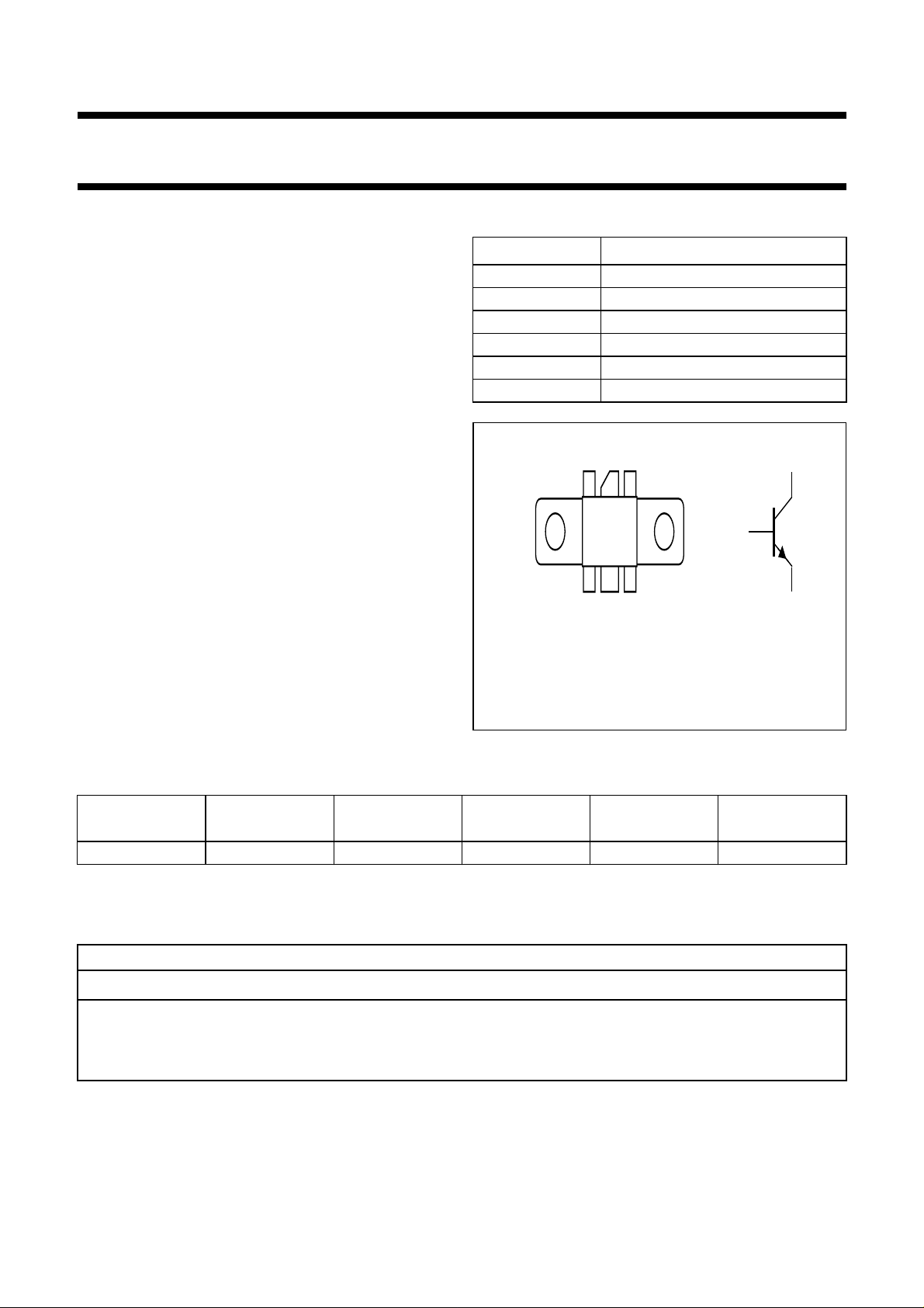
DESCRIPTION
NPN silicon planar transistor in a SOT171A 6-lead
rectangular flange package, with a ceramic cap. The
transistor delivers a P
860 MHz and a supply voltage of 25 V.
= 3 W in class-A operation at
o sync
PINNING SOT171A
PIN DESCRIPTION
1 emitter
2 emitter
3 base
4 collector
5 emitter
6 emitter
handbook, halfpage
12345
Top view
6
c
b
e
MAM141
Fig.1 Simplified outline and symbol.
QUICK REFERENCE DATA
RF performance at T
MODE OF
OPERATION
CW class-A 860 25 1.1 ≥3
Note
1. Three-tone test signal (−8, −16, and −10 dB); d
Product and environmental safety - toxic materials
This product contains beryllium oxide. The product is entirely safe provided that the BeO disc is not damaged.
All persons who handle, use or dispose of this product should be aware of its nature and of the necessary safety
precautions. After use, dispose of as chemical or special waste according to the regulations applying at the location of
the user. It must never be thrown out with the general or domestic waste.
=25°C in a common emitter test circuit.
h
f
(MHz)
V
(V)
CE
= −63 dB.
im
WARNING
I
CQ
(A)
P
o sync
(W)
(1)
G
(dB)
≥9
p
(1)
1996 Jul 16 2
Philips Semiconductors Product specification
UHF linear power transistor BLW898
LIMITING VALUES
In accordance with the Absolute Maximum Rating System (IEC 134).
SYMBOL PARAMETER CONDITIONS MIN. MAX. UNIT
V
CBO
V
CEO
V
EBO
I
C
I
C(AV)
P
tot
T
stg
T
j
THERMAL CHARACTERISTICS
SYMBOL PARAMETER CONDITIONS VALUE UNIT
R
th j-mb
R
th mb-h
collector-base voltage open emitter − 60 V
collector-emitter voltage open base − 28 V
emitter-base voltage open collector − 2.5 V
collector current (DC) − 3.7 A
average collector current − 3.7 A
total power dissipation up to Tmb=70°C − 44 W
storage temperature −65 +150 °C
operating junction temperature − 200 °C
thermal resistance from junction to
P
= 44 W; Tmb=70°C 3 K/W
tot
mounting-base
thermal resistance from
0.3 K/W
mounting-base to heatsink
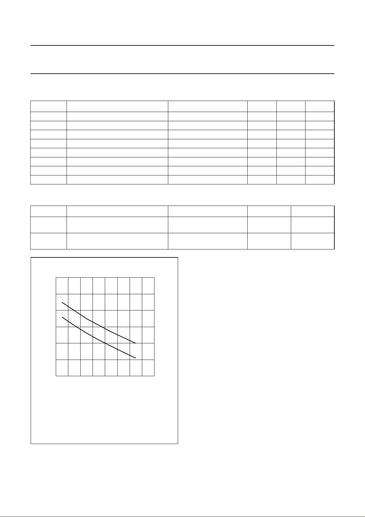
120
handbook, halfpage
P
tot
(W)
80
40
0
0
(1) Continuous operation
(2) Short-time operation during mismatch.
(2)
(1)
40 80 160
Fig.2 Power derating curve.
120
MGD531
Tmb °C
1996 Jul 16 3
Philips Semiconductors Product specification
UHF linear power transistor BLW898
CHARACTERISTICS
T
=25°C unless otherwise specified.
j
SYMBOL PARAMETER CONDITIONS MIN. TYP. MAX. UNIT
V
(BR)CBO
V
(BR)CEO
V
(BR)EBO
I
CBO
I
CEO
h
FE
C
c
C
re
collector-base breakdown voltage IC= 15 mA; IE=0 60 −−V
collector-emitter breakdown voltage IC= 30 mA; IB=0 28 −−V
emitter-base breakdown voltage IE= 0.6 mA; IC= 0 2.5 −−V
collector-base leakage current VBE= 0; VCB=28V −−1.5 mA
collector-emitter leakage current VCE=20V −−3mA
DC current gain VCE= 25 V; IC= 1.1 A 30 − 140
collector capacitance VCB= 25 V; IE=ie=0;
− 18 − pF
f = 1 MHz
feedback capacitance VCB= 25 V; IC= 0; f = 1 MHz − 11 − pF
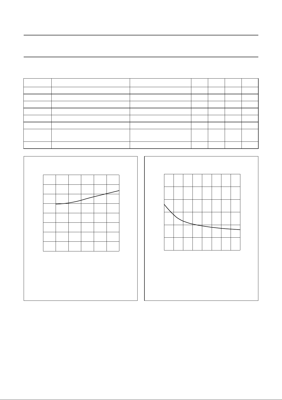
160
handbook, halfpage
h
FE
120
80
40
0
01
VCE= 25V; tp= 500 µs; δ =<1%.
2
MGD532
IC (A)
Fig.3 DC current gain as a function of collector
current; typical values.
30
MGD533
VCB (V)
60
handbook, halfpage
C
c
(pF)
40
20
0
3
0
IE=ie= 0; f = 1 MHz.
10 20 40
Fig.4 Collector capacitance as a function of
collector-base voltage; typical values.
1996 Jul 16 4
 Loading...