

Philips BLW50F Datasheet

DISCRETE SEMICONDUCTORS
DATA SH EET
BLW50F
HF/VHF power transistor
Product specification
August 1986
Philips Semiconductors Product specification
HF/VHF power transistor BLW50F
DESCRIPTION
N-P-N silicon planar epitaxial
transistor primarily intended for use in
It has a 3/8" flange envelope with a
ceramic cap. All leads are isolated
from the flange.
class-A, AB and B operated, industrial
and military transmitters in the h.f.
and v.h.f. band. Resistance
stabilization provides protection
against device damage at severe load
mismatch conditions. Matched
hFEgroups are available on request.
QUICK REFERENCE DATA
R.F. performance
MODE OF OPERATION V
CE
V
f
MHz
P
W
L
G
p
dB
η
dt
%
I
I
C
C(ZS)
A
mA
d
dB
3
s.s.b. (class-A) 45 1,6 - 28 0 - 16 (P.E.P.) > 19,5 − 1,2 −<−40 70
(1)
s.s.b. (class-AB) 50 1,6 - 28 10 - 65 (P.E.P.) typ. 18 typ. 45
1,45 50 typ. −30 25
Note
1. At 65W P.E.P.
T
°C
h
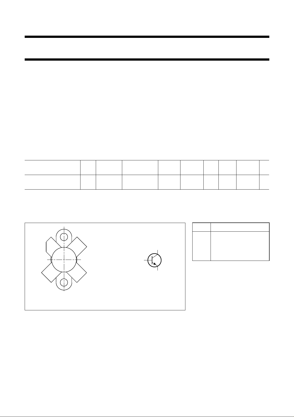
PIN CONFIGURATION
PINNING - SOT123
PIN DESCRIPTION
lfpage
1
23
4
handbook, halfpage
MSB057
MBB012
c
b
e
1 collector
2 emitter
3 base
4 emitter
Fig.1 Simplified outline and symbol.
PRODUCT SAFETY This device incorporates beryllium oxide, the dust of which is toxic. The device is entirely
safe provided that the BeO disc is not damaged.
August 1986 2

Philips Semiconductors Product specification
HF/VHF power transistor BLW50F
RATINGS
Limiting values in accordance with the Absolute Maximum System (IEC 134)
Collector-emitter voltage (V
peak value V
Collector-emitter voltage (open base) V
Emitter-base voltage (open collector) V
Collector current (average) I
Collector current (peak value); f > 1 MHz I
D.C. and r.f. (f > 1 MHz) power dissipation; T
Storage temperature T
Operating junction temperature T
BE
= 0)
CESM
CEO
EBO
C(AV)
CM
= 25 °CP
mb
tot;Prf
stg
j
max. 110 V
max. 55 V
max. 4 V
max. 2,5 A
max. 7,5 A
max. 94 W
−65 to + 150 °C
max. 200 °C
10
handbook, halfpage
I
C
(A)
1
−1
10
1 10 10
Th = 70 °C
VCE (V)
Fig.2 D.C. SOAR.
MGP466
Tmb = 25 °C
150
handbook, halfpage
P
rf
(W)
100
ΙΙ
50
Ι
2
0
0
I Continuous d.c. and r.f. operation
II Short-time operation during mismatch
50
Th (°C)
MGP467
100
Fig.3 Power derating curves vs. temperature.
THERMAL RESISTANCE
(dissipation = 54 W; T
=86°C, i.e. Th=70°C)
mb
From junction to mounting base
(d.c. and r.f. dissipation) R
From mounting base to heatsink R
August 1986 3
th j-mb
th mb-h
= 2,1 K/W
= 0,3 K/W

Philips Semiconductors Product specification
HF/VHF power transistor BLW50F
CHARACTERISTICS
T
=25°C
j
Collector-emitter breakdown voltage
V
= 0; IC= 25 mA V
BE
Collector-emitter breakdown voltage
open base; IC= 100 mA V
Emitter-base breakdown voltage
open collector; IE= 10 mA V
Collector cut-off current
VBE= 0; VCE= 55 V I
Second breakdown energy; L = 25 mH; f = 50 Hz
open base E
R
=10Ω E
BE
D.C. current gain
(1)
IC= 1,2 A; VCE=5 V h
D.C. current gain ratio of matched devices
(1)
IC= 1,2 A; VCE=5 V h
Collector-emitter saturation voltage
(1)
IC= 3,0 A; IB= 0,6 A V
Transition frequency at f = 100 MHz
(1)
−IE= 1,2 A; VCB= 45 V f
= 4,0 A; VCB= 45 V f
−I
E
Collector capacitance at f = 1 MHz
IE=Ie= 0; VCB= 45 V C
Feedback capacitance at f = 1 MHz
I
= 50 mA; VCE= 45 V C
C
Collector-flange capacitance C
(BR) CES
(BR) CEO
(BR)EBO
CES
SBO
SBR
FE
FE1/hFE2
CEsat
T
T
c
re
cf
> 110 V
> 55 V
> 4V
< 10 mA
> 8mJ
> 8mJ
typ. 25
15 to 100
< 1,2
typ. 1,2 V
typ. 490 MHz
typ. 540 MHz
typ. 53 pF
typ. 35 pF
typ. 2 pF
Note
1. Measured under pulse conditions: t
≤ 200 µs; δ≤0,02.
p
August 1986 4
 Loading...