

Philips BLW30 Datasheet

DISCRETE SEMICONDUCTORS
DATA SH EET
BLW30
VHF power transistor
Product specification
September 1991

Philips Semiconductors Product specification
VHF power transistor BLW30
FEATURES
• Emitter-ballasting resistors for an
optimum temperature profile
• Excellent reliability
• Withstands full load mismatch.
DESCRIPTION
NPN silicon planar epitaxial transistor
encapsulated in a 4-lead
3
⁄8inch
SOT120 capstan envelope with a
ceramic cap. It is designed for
common emitter, class-B operation
mobile VHF transmitters with a supply
voltage of 12.5 V. All leads are
isolated from the stud.
PINNING - SOT120
PIN DESCRIPTION
1 collector
2 emitter
3 base
4 emitter
QUICK REFERENCE DATA
RF performance at T
MODE OF
OPERATION
= 25 °C in a common emitter test circuit.
mb
f
(MHz)
V
(V)
CE
P
(W)
L
G
P
(dB)
η
(%)
c.w. class-B 175 12.5 30 > 10 > 55
WARNING
Product and environmental safety - toxic materials
This product contains beryllium oxide. The product is entirely safe provided
that the BeO disc is not damaged. All persons who handle, use or dispose of
this product should be aware of its nature and of the necessary safety
precautions. After use, dispose of as chemical or special waste according to
the regulations applying at the location of the user. It must never be thrown
out with the general or domestic waste.
PIN CONFIGURATION
alfpage
4
31
handbook, halfpage
b
c
C
MBB012
2
MSB056
Fig.1 Simplified outline and symbol.
e
September 1991 2
Philips Semiconductors Product specification
VHF power transistor BLW30
LIMITING VALUES
In accordance with the Absolute Maximum System (IEC 134).
SYMBOL PARAMETER CONDITIONS MIN. MAX. UNIT
V
CBO
V
CEO
V
EBO
I
C,IC(AV)
I
CM
P
tot
T
stg
T
j
collector-base voltage open emitter − 36 V
collector-emitter voltage open base − 16 V
emitter-base voltage open collector − 3V
collector current DC or average value − 6A
collector current peak value
− 18 A
f > 1 MHz
total power dissipation RF operation;
− 100 W
f > 1 MHz;
Tmb=25°C
storage temperature range −65 150 °C
junction operating temperature − 200 °C
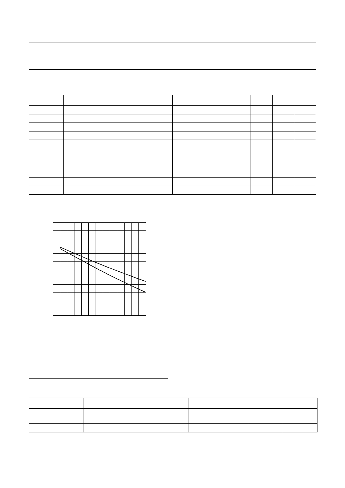
120
handbook, halfpage
P
tot
(W)
100
II
80
60
40
20
0
(I) Continuous RF operation (f> 1 MHz).
(II) Shorttime operation during mismatch
(f > 1 MHz).
I
020406080100120
Fig.2 Power/temperature derating curve.
MRA382
o
T ( C)
h
THERMAL RESISTANCE
SYMBOL PARAMETER CONDITIONS MAX. UNIT
R
th j-mb(RF)
from junction to mounting base P
= 100 W;
tot
1.75 K/W
Tmb=25°C
R
th mb-h
from mounting base to heatsink 0.45 K/W
September 1991 3
Philips Semiconductors Product specification
VHF power transistor BLW30
CHARACTERISTICS
T
= 25 °C.
j
SYMBOL PARAMETER CONDITIONS MIN. TYP. MAX. UNIT
V
(BR)CBO
V
(BR)CEO
V
(BR)EBO
I
CES
h
FE
f
T
C
c
C
re
C
c-s
collector-base breakdown voltage open emitter;
Ic= 10 mA
collector-emitter breakdown voltage open base;
Ic= 25 mA
emitter-base breakdown voltage open collector;
IE= 2 mA
collector-emitter leakage current VBE=0;
VCE= 16 V
DC current gain VCE=5 V;
IC=4 A
transition frequency VCE= 12.5 V;
IE= 4 A;
f = 500 MHz
collector capacitance VCB= 12.5 V;
IE=Ie=0;
f = 1 MHz
feedback capacitance VCE= 12.5 V;
IC=0;
f = 1 MHz
collector-stud capacitance f = 1 MHz − 2 − pF
36 −−V
16 −−V
3 −−V
−−10 mA
25 35 −
− 1.6 − GHz
− 90 100 pF
− 60 70 pF
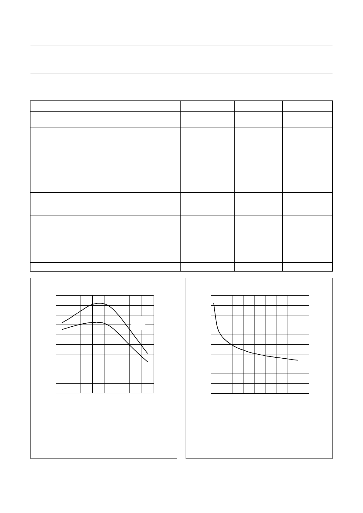
VCE=
12.5 V
I (A)
C
MRA378
50
handbook, halfpage
h
FE
40
30
20
10
0
0 4 8 12 16
V = 5 V
CE
Fig.3 DC current gain as a function of collector
current, typical values.
250
handbook, halfpage
C
c
(pF)
200
150
100
50
0
0 4 8 12 16
IE=ie= 0; f = 1 MHz.
V (V)
Fig.4 Collector capacitance as a function of
collector-base voltage, typical values.
MRA374.1
CB
September 1991 4
 Loading...