

Philips BLV98CE Datasheet

DISCRETE SEMICONDUCTORS
DATA SH EET
BLV98CE
UHF power transistor
Product specification
March 1993
Philips Semiconductors Product specification
UHF power transistor BLV98CE
FEATURES
• Internal input matching to achieve high power gain
• Implanted ballasting resistors an for optimum
temperature profile
• Gold metallization ensures excellent reliability
QUICK REFERENCE DATA
RF performance up to T
=25°C in a common emitter class-AB circuit.
h
MODE OF OPERATION f (MHz) V
c.w. class-AB 960 24 15 > 7.5 > 50
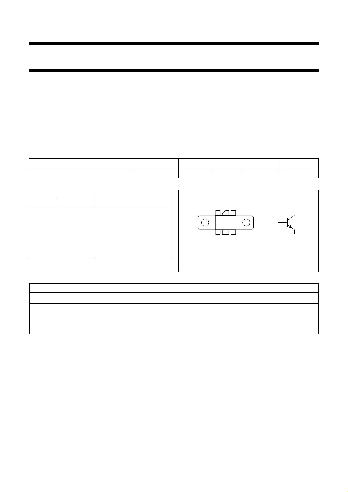
PINNING - SOT171A
PIN SYMBOL DESCRIPTION
1 e emitter
2 e emitter
3 b base
4 c collector
5 e emitter
6 e emitter
DESCRIPTION
NPN silicon planar epitaxial transistor in an SOT-171
envelope, intended for common emitter, class-AB
operation in radio transmitters for the 960 MHz
communications band. The transistor has a 6-lead flange
envelope, with a ceramic cap. All leads are isolated from
the flange.
(V) PL(W) GP(dB) ηc(%)
CE
handbook, halfpage
Top view
12345
6
b
MAM141
c
e
Fig.1 Simplified outline and symbol.
WARNING
Product and environmental safety - toxic materials
This product contains beryllium oxide. The product is entirely safe provided that the BeO disc is not damaged.
All persons who handle, use or dispose of this product should be aware of its nature and of the necessary safety
precautions. After use, dispose of as chemical or special waste according to the regulations applying at the location of
the user. It must never be thrown out with the general or domestic waste.
March 1993 2
Philips Semiconductors Product specification
UHF power transistor BLV98CE
LIMITING VALUES
Limiting values in accordance with the Absolute Maximum System (IEC 134)
SYMBOL PARAMETER CONDITIONS MIN. MAX. UNIT
V
CBO
V
CEO
V
EBO
I
C
I
CM
P
tot
T
stg
T
j
THERMAL RESISTANCE
collector base voltage open emitter − 50 V
collector emitter voltage open base − 27 V
emitter base voltage open collector − 3.5 V
collector current DC or average − 1.5 A
collector current peak value
− 4.5 A
f > 1 MHz
total power dissipation f > 1 MHz
− 40 W
Tmb=25°C
storage temperature −65 150 °C
operating junction temperature − 200 °C
SYMBOL PARAMETER CONDITIONS TYP. MAX. UNIT
R
thj-mb
R
th mb-h
10
handbook, halfpage
I
C
(A)
1
−1
10
from junction to mounting base (RF) − 4.4 K/W
from mounting base to heatsink − 0.4 K/W
MDA449
Tmb = 25 °C
Th = 70 °C
110
V
(V)
CE
2
10
60
handbook, halfpage
P
tot
(W)
40
20
0
0
(1) DC or RF operation
(2) short-term operation during mismatch
40
(2)
(1)
80 160120
MDA450
Th (°C)
Fig.2 DC SOAR.
March 1993 3
Fig.3 Power/temperature derating.
Philips Semiconductors Product specification
UHF power transistor BLV98CE
CHARACTERISTICS
at T
=25°C unless otherwise stated.
j
SYMBOL PARAMETER CONDITIONS MIN. TYP. MAX. UNIT
V
(BR)CBO
V
(BR)CEO
V
(BR)EBO
I
CES
h
FE
C
c
C
re
C
cf
collector-base breakdown voltage open emitter
IC= 25 mA
collector-emitter breakdown voltage open base
IC= 50 mA
emitter-base breakdown voltage open collector
IE= 5 mA
collector leakage current VBE=0
VCE= 27 V
DC current gain IC=1 A
VCE= 20 V
collector capacitance at f = 1 MHz IE=Ie=0
VCB= 24 V
feedback capacitance at f = 1 MHz IC=0
VCE= 24 V
collector-flange capacitance − 2 − pF
50 −−V
27 −−V
3.5 −−V
−− 5mA
15 −−
− 23 − pF
− 14 − pF
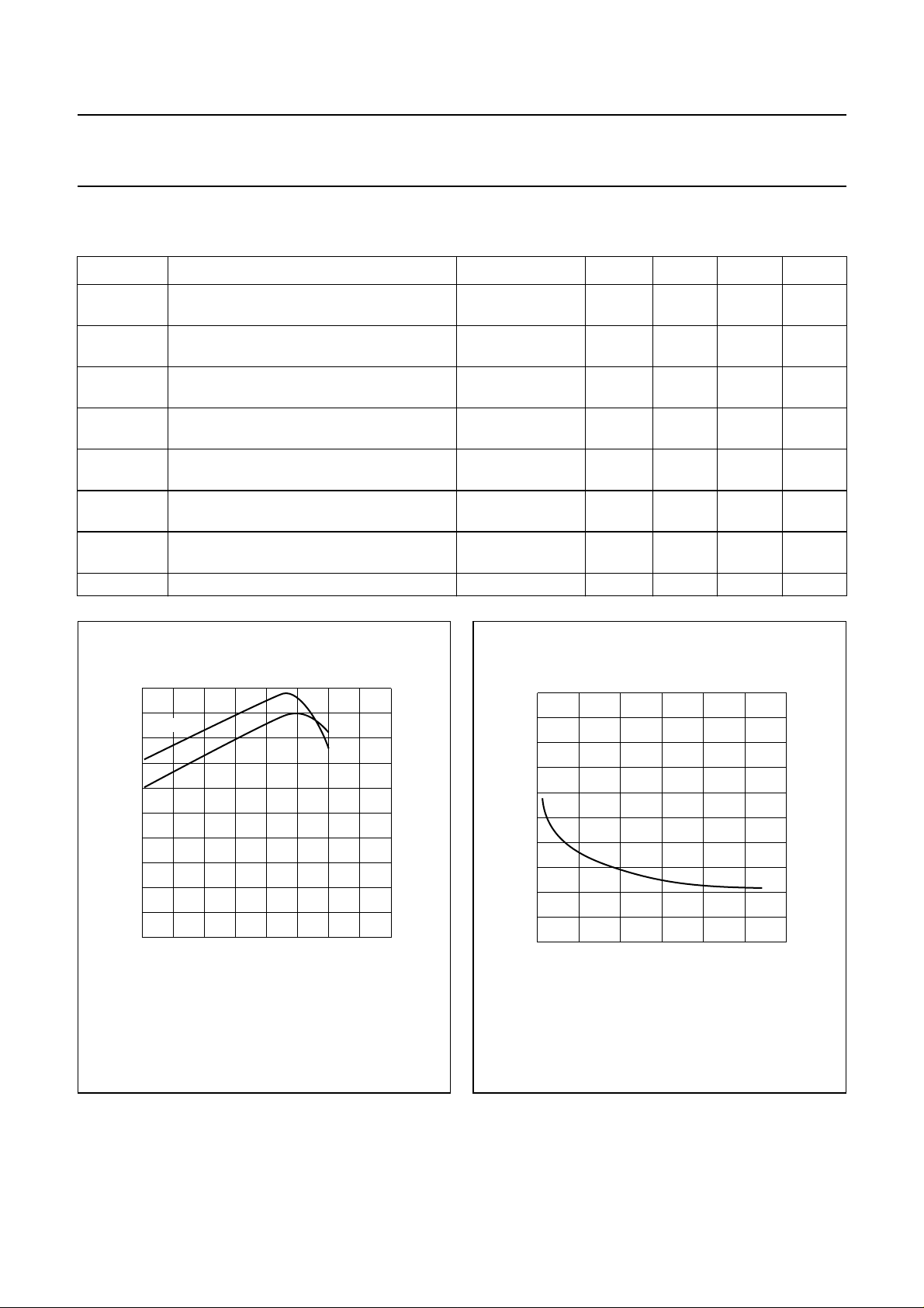
100
handbook, halfpage
h
FE
V
CE
80
60
40
20
0
012
= 24 V
20 V
MDA451
3
IC (A)
Fig.4 DC current gain as a function of collector
current; typical values.
100
handbook, halfpage
C
c
(pF)
80
60
40
20
4
0
010
20 30
MDA452
V
(V)
CB
Fig.5 Output capacitance as a function of VCB;
typical values.
March 1993 4
 Loading...