

Philips BLV950 Datasheet

DISCRETE SEMICONDUCTORS
DATA SH EET
BLV950
UHF push-pull power transistor
Product specification
Supersedes data of 1996 Jan 26
1997 Oct 27
Philips Semiconductors Product specification
UHF push-pull power transistor BLV950
FEATURES
• Internal input and output matching for easy matching,
high gain and efficiency
• Poly-silicon emitter ballasting resistors for an optimum
temperature profile
• Gold metallization ensures excellent reliability.
APPLICATIONS
• Base station transmitters in the 800 to 960 MHz range.
DESCRIPTION
Two NPN silicon planar epitaxial transistors in push-pull
configuration, intended for linear common emitter
class-AB operation. The transistors are encapsulated in a
4-lead SOT262A2 flange package with 2 ceramic caps.
The flange provides the common emitter connection for
both transistors.
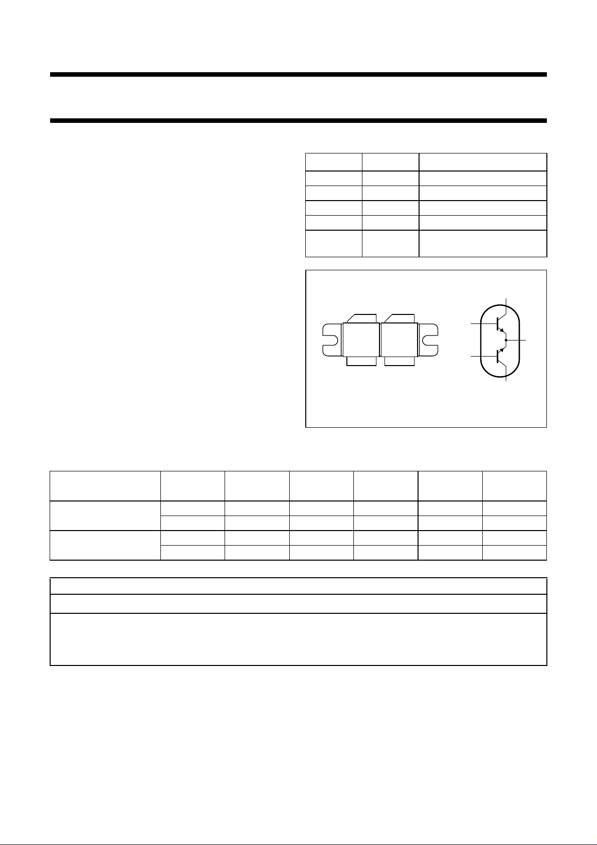
PINNING - SOT262A2
PIN SYMBOL DESCRIPTION
1 c1 collector 1
2 c2 collector 2
3 b1 base 1
4 b2 base 2
5 e common emitter; connected
to flange
handbook, halfpage
12
b1
55
34
Top view
b2
MAM031
Fig.1 Simplified outline and symbol.
c1
e
c2
QUICK REFERENCE DATA
RF performance at T
MODE OF OPERATION
=25°C in a common emitter push-pull test circuit.
h
f
(MHz)
V
(V)
CE
P
(W)
L
G
(dB)
p
η
C
(%)
d
3
(dBc)
CW, class-AB 900 26 150 ≥8 ≥45 −
960 26 150 ≥7.5 ≥45 −
2-tone, class-AB 900 26 150 (PEP) ≥8.5 ≥35 ≤−30
960 26 150 (PEP) ≥8 ≥35 ≤−30
WARNING
Product and environmental safety - toxic materials
This product contains beryllium oxide. The product is entirely safe provided that the BeO discs are not damaged.
All persons who handle, use or dispose of this product should be aware of its nature and of the necessary safety
precautions. After use, dispose of as chemical or special waste according to the regulations applying at the location of
the user. It must never be thrown out with the general or domestic waste.
1997 Oct 27 2

Philips Semiconductors Product specification
UHF push-pull power transistor BLV950
LIMITING VALUES
In accordance with the Absolute Maximum Rating System (IEC 134).
SYMBOL PARAMETER CONDITIONS MIN. MAX. UNIT
Per transistor section
V
CBO
V
CEO
V
EBO
I
C
I
C(AV)
P
tot
T
stg
T
j
THERMAL CHARACTERISTICS
collector-base voltage open emitter − 70 V
collector-emitter voltage open base − 30 V
emitter-base voltage open collector − 3V
collector current (DC) − 12 A
average collector current − 12 A
total power dissipation (DC) Tmb=25°C − 340 W
storage temperature −65 +150 °C
operating junction temperature − 200 °C
SYMBOL PARAMETER CONDITIONS MAX. UNIT
R
th j-mb
thermal resistance from junction to
P
= 340 W; Tmb=25°C; note 1 0.52 K/W
tot
mounting base
R
th mb-h
thermal resistance from mounting
0.15 K/W
base to heatsink
Note
1. Total device; both sections equally loaded; thermal resistance is determined under specified RF operating
conditions.
1997 Oct 27 3
Philips Semiconductors Product specification
UHF push-pull power transistor BLV950
CHARACTERISTICS
T
=25°C unless otherwise specified.
j
SYMBOL PARAMETER CONDITIONS MIN. TYP. MAX. UNIT
Per transistor section
V
(BR)CBO
V
(BR)CEO
V
(BR)EBO
I
CES
h
FE
C
c
Notes
1. Measured under pulse conditions: t
2. Value Cc is that of the die only, it is not measurable because of internal matching network.
collector-base breakdown voltage open emitter; IC=60mA 70 −−V
collector-emitter breakdown voltage open base; IC= 150 mA 30 −−V
emitter-base breakdown voltage open collector; IE= 3 mA 3 −−V
collector leakage current VBE= 0; VCE=28V −−5mA
DC current gain VCE= 10 V; IC= 4.5 A; note 1 30 − 120
collector capacitance VCB= 26 V; IE=ie=0;
− 75 − pF
f = 1 MHz; note 2
≤ 300 µs; δ≤0.01.
p
80
handbook, halfpage
h
FE
60
40
20
0
04 81216
Measured under pulsed conditions; tp≤ 300µs; δ≤0.01.
(1) VCE=26V.
(2) VCE=10V.
(1)
(2)
MLD256
IC(A)
Fig.2 DC current gain as a function of collector
current; typical values.
300
handbook, halfpage
C
c
(pF)
200
100
0
0102030 5040
Value Cc is that of the die only, it is not measurable because of
internal matching network.
= 0; f = 1 MHz.
I
E=ie
V (V)
Fig.3 Collector capacitance as a function of
collector-base voltage; typical values.
MLD257
CB
1997 Oct 27 4
Philips Semiconductors Product specification
UHF push-pull power transistor BLV950
APPLICATION INFORMATION
RF performance at T
=25°C in a common emitter push-pull test circuit; R
h
th mb-h
= 0.15 K/W.
MODE OF OPERATION
f
(MHz)
CW, class-AB 900 26 2 × 100 150 ≥8
960 26 2 × 100 150 ≥7.5
2-tone, class-AB note 1 26 2 × 100 150 (PEP) ≥8.5
note 2 26 2 × 100 150 (PEP) ≥8
V
(V)
CE
I
CQ
(mA)
P
(W)
L
G
p
(dB)
typ. 9
typ. 8.5
typ. 9.5
typ. 9
η
C
(%)
≥45
typ. 50
≥45
typ. 50
≥35
typ. 40
≥35
typ. 40
d
3
(dBc)
−
−
≤−28
typ. −31
≤−30
typ. −33
Notes
1. f
= 900.0 MHz; f2= 900.1 MHz.
1
2. f1= 960.0 MHz; f2= 960.1 MHz.
Ruggedness in class-AB operation
The BLV950 is capable of withstanding a load mismatch corresponding to VSWR =2:1 through all phases under the
conditions: P
= 150 W; f = 960 MHz; VCE= 26 V; ICQ=2×100 mA; Th=25°C; R
L
= 0.15 K/W and also a load
th mb-h
mismatch of VSWR = 5 : 1 through all phases at PL= 150 W (PEP) and f1= 960.0 MHz and f2= 960.1 MHz.
12
handbook, halfpage
G
p
(dB)
8
MLD258
60
η
C
G
p
η
C
(%)
40
200
handbook, halfpage
P
L
(W)
150
100
MLD259
4
0
0 50 100 150 200
VCE= 26 V; ICQ=2×100 mA; f = 960 MHz.
P (W)
L
20
0
Fig.4 Power gain and efficiency as functions of
load power; typical values.
1997 Oct 27 5
50
0
0102030
VCE= 26 V; ICQ=2×100 mA; f = 960 MHz.
P (W)
i
Fig.5 Load power as a function of input power;
typical values.
 Loading...