

Philips BLV92 Datasheet

DISCRETE SEMICONDUCTORS
DATA SH EET
BLV92
UHF power transistor
Product specification
March 1993
Philips Semiconductors Product specification
UHF power transistor BLV92
DESCRIPTION
N-P-N silicon planar epitaxial transistor primarily intended
for use in mobile radio transmitters in the 900 MHz
communications band.
QUICK REFERENCE DATA
R.F. performance at T
MODE OF OPERATION V
narrow band; c.w.
=25°C in a common-emitter class-B test circuit
h
CE
V
f
MHz
12,5 900 4 > 7,5 > 50
9,6 900 3 typ. 7,3 typ. 56
PINNING - SOT171A
PIN SYMBOL DESCRIPTION
1 e emitter
2 e emitter
3 b base
4 c collector
5 e emitter
6 e emitter
FEATURES
• multi-base structure and emitter-ballasting resistors for
an optimum temperature profile
• internal input matching to achieve an optimum wideband
capability and high power gain
• gold metallization ensures excellent reliability.
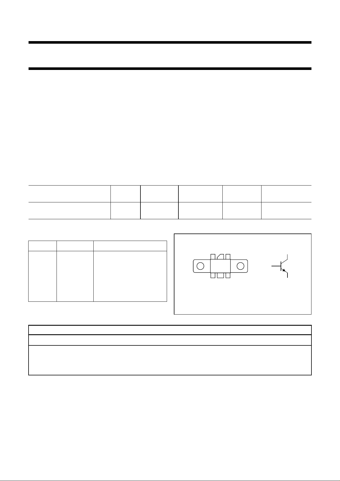
The transistor has a 6-lead flange envelope with a ceramic
cap (SOT-171). All leads are isolated from the flange.
P
L
W
handbook, halfpage
Top view
12345
G
P
dB
6
MAM141
η
C
%
c
b
e
Fig.1 Simplified outline and symbol.
WARNING
Product and environmental safety - toxic materials
This product contains beryllium oxide. The product is entirely safe provided that the BeO disc is not damaged.
All persons who handle, use or dispose of this product should be aware of its nature and of the necessary safety
precautions. After use, dispose of as chemical or special waste according to the regulations applying at the location of
the user. It must never be thrown out with the general or domestic waste.
March 1993 2
Philips Semiconductors Product specification
UHF power transistor BLV92
RATINGS
Limiting values in accordance with the Absolute Maximum System (IEC 134)
Collector-base voltage (open emitter)
peak value V
Collector-emitter voltage (open base) V
Emitter-base voltage (open collector) V
Collector current
d.c. or average I
(peak value); f > 1 MHz I
Total power dissipation
at T
=94°CP
mb
= 94 °C; f > 1 MHz P
at T
mb
Storage temperature T
Operating junction temperature T
CBOM
CEO
EBO
C
CM
tot(dc)
tot(rf)
stg
j
max. 36 V
max. 16 V
max. 3 V
max. 0,8 A
max. 2,4 A
max. 9 W
max. 12 W
−65 to + 150 °C
max. 200 °C
CE
(V)
MDA408
20
handbook, halfpage
P
tot
(W)
16
12
8
4
2
10
0
0
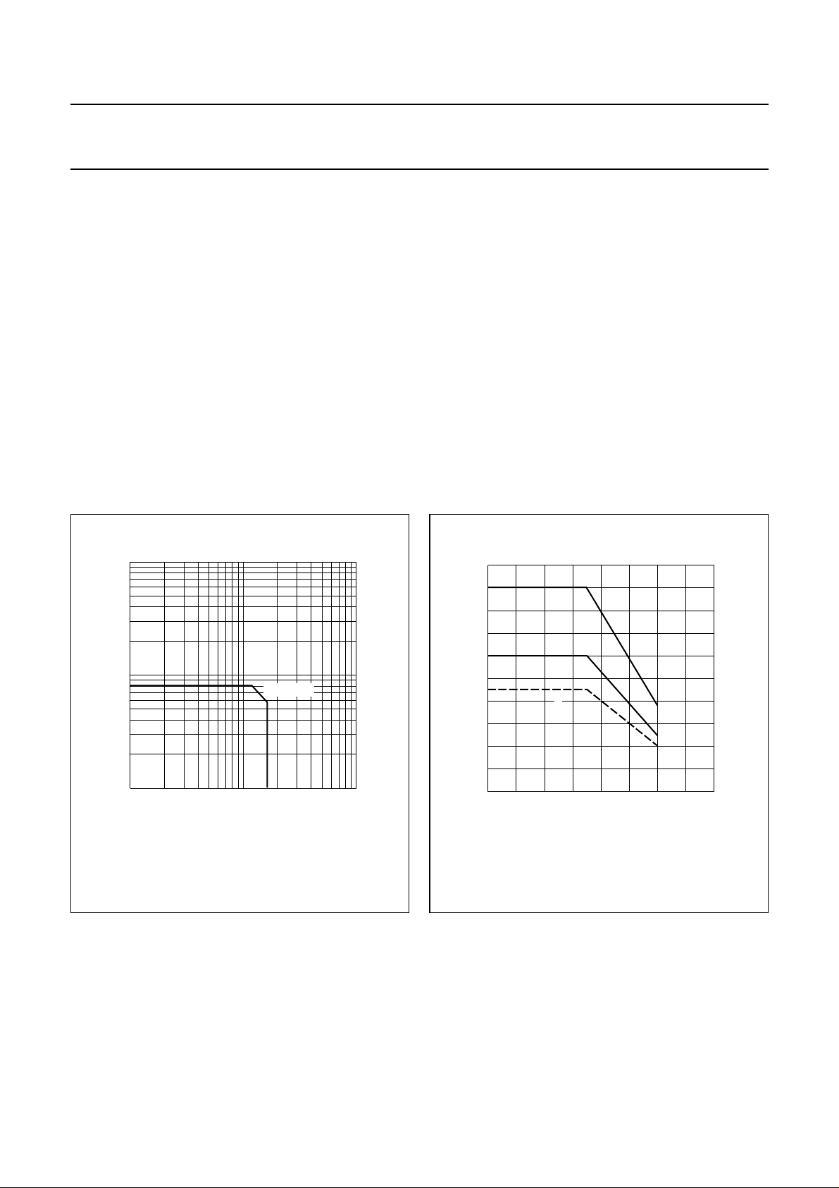
I Continuous operation
II Continuous operation (f > 1 MHz)
III Short-time operation during mismatch; (f > 1 MHz)
III
II
I
50 100
Fig.3 Power/temperature derating curves.
10
handbook, halfpage
I
C
(A)
1
−1
10
110
R
= 0,4 K/W.
th mb-h
Th = 90 °C
V
Fig.2 D.C. SOAR.
THERMAL RESISTANCE
Dissipation = 6 W; T
= 128 °C
mb
From junction to mounting base
(d.c. dissipation) R
(r.f. dissipation) R
From mounting base to heatsink R
th j-mb(dc)
th j-mb(rf)
th mb-h
MDA409
Th (°C)
200
150
max. 12 K/W
max. 9 K/W
max. 0,4 K/W
March 1993 3

Philips Semiconductors Product specification
UHF power transistor BLV92
CHARACTERISTICS
T
=25°C unless otherwise specified
j
Collector-base breakdown voltage, open emitter; I
Collector-emitter breakdown voltage, open base; I
Emitter-base breakdown voltage, open collector; I
Collector cut-off current, V
= 0; VCE= 16 V I
BE
Second breakdown energy, L = 25 mH; f = 50 Hz; R
D.C. current gain, I
Transition frequency at f = 500 MHz
Collector capacitance at f = 1 MHz, I
Feed-back capacitance at f = 1 MHz, I
= 0,6 A; VCE=10V h
C
(1)
, −IE= 0,6 A; VCE= 12,5 V f
= ie=0;VCB= 12,5 V C
E
= 0; VCE= 12,5 V C
C
Collector-flange capacitance C
Note
1. Measured under pulse conditions: t
=50µs; δ<1%.
p
=10mA V
C
=20mA V
C
= 1 mA V
E
=10Ω E
BE
(BR)CBO
(BR)CEO
(BR)EBO
CES
SBR
FE
T
c
re
cf
> 36 V
> 16 V
> 3V
< 5mA
> 1mJ
> 25
typ. 4 GHz
typ. 8 pF
typ. 5 pF
typ. 2 pF
100
handbook, halfpage
h
FE
80
60
40
20
0
02
12.5 V
V
= 10 V
CE
0.4 0.8 1.2
1.6
IC (A)
Fig.4 Tj=25°C; typical values.
MDA410
handbook, halfpage
5
f
T
(GHz)
4
3
2
1
0
−0.4 −0.8 −1.2
0 −2
−1.6
Fig.5 VCB= 12,5 V; f = 500 MHz; Tj=25°C;
typical values.
MDA411
IE (A)
March 1993 4
 Loading...