

Philips blv910 DATASHEETS

DISCRETE SEMICONDUCTORS
DATA SH EET
BLV910
UHF power transistor
Product specification
Philips Semiconductors
1995 Apr 11
Philips Semiconductors Product specification
UHF power transistor BLV910
FEATURES
• Internal input matching to achieve high power gain and
easy design of wideband circuits
• Emitter ballasting resistors for an optimum temperature
profile
• Gold metallization ensures excellent reliability.
APPLICATIONS
• Base station transmitters in the 820 to 960 MHz range.
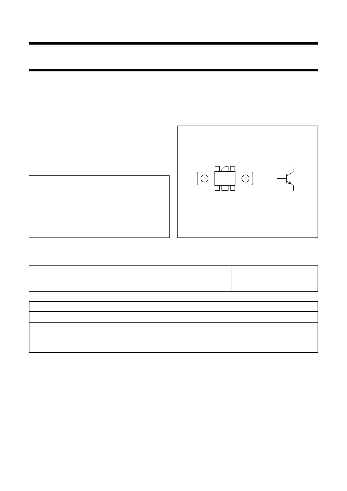
PINNING - SOT171
PIN SYMBOL DESCRIPTION
1 e emitter
2 e emitter
3 b base
4 c collector
5 e emitter
6 e emitter
DESCRIPTION
NPN silicon planar epitaxial transistor intended for
common emitter class-AB operation. The transistor is
encapsulated in a 6-lead SOT171 flange envelope with a
ceramic cap. All leads are isolated from the flange.
handbook, halfpage
Top view
12345
6
b
MAM141
c
e
Fig.1 Simplified outline and symbol.
QUICK REFERENCE DATA
RF performance at T
MODE OF OPERATION
= 25 °C in a common emitter test circuit.
mb
f
(MHz)
V
(V)
CE
P
(W)
L
G
p
(dB)
η
(%)
C
CW, class-AB 960 26 10 ≥11 ≥ 55
WARNING
Product and environmental safety - toxic materials
This product contains beryllium oxide. The product is entirely safe provided that the BeO disc is not damaged.
All persons who handle, use or dispose of this product should be aware of its nature and of the necessary safety
precautions. After use, dispose of as chemical or special waste according to the regulations applying at the location of
the user. It must never be thrown out with the general or domestic waste.
1995 Apr 11 2
Philips Semiconductors Product specification
UHF power transistor BLV910
LIMITING VALUES
In accordance with the Absolute Maximum Rating System (IEC 134).
SYMBOL PARAMETER CONDITIONS MIN. MAX. UNIT
V
CBO
V
CEO
V
EBO
I
C
I
C(AV)
P
tot
T
stg
T
j
THERMAL CHARACTERISTICS
SYMBOL PARAMETER CONDITIONS VALUE UNIT
R
th j-mb
R
th mb-h
collector-base voltage open emitter − 70 V
collector-emitter voltage open base − 30 V
emitter-base voltage open collector − 3V
collector current (DC) − 1.5 A
average collector current − 1.5 A
total power dissipation up to Tmb=25°C − 30 W
storage temperature −65 +150 °C
operating junction temperature − 200 °C
thermal resistance from junction to
P
= 30 W; Tmb=25°C 5.85 K/W
tot
mounting base
thermal resistance from mounting
0.4 K/W
base to heatsink
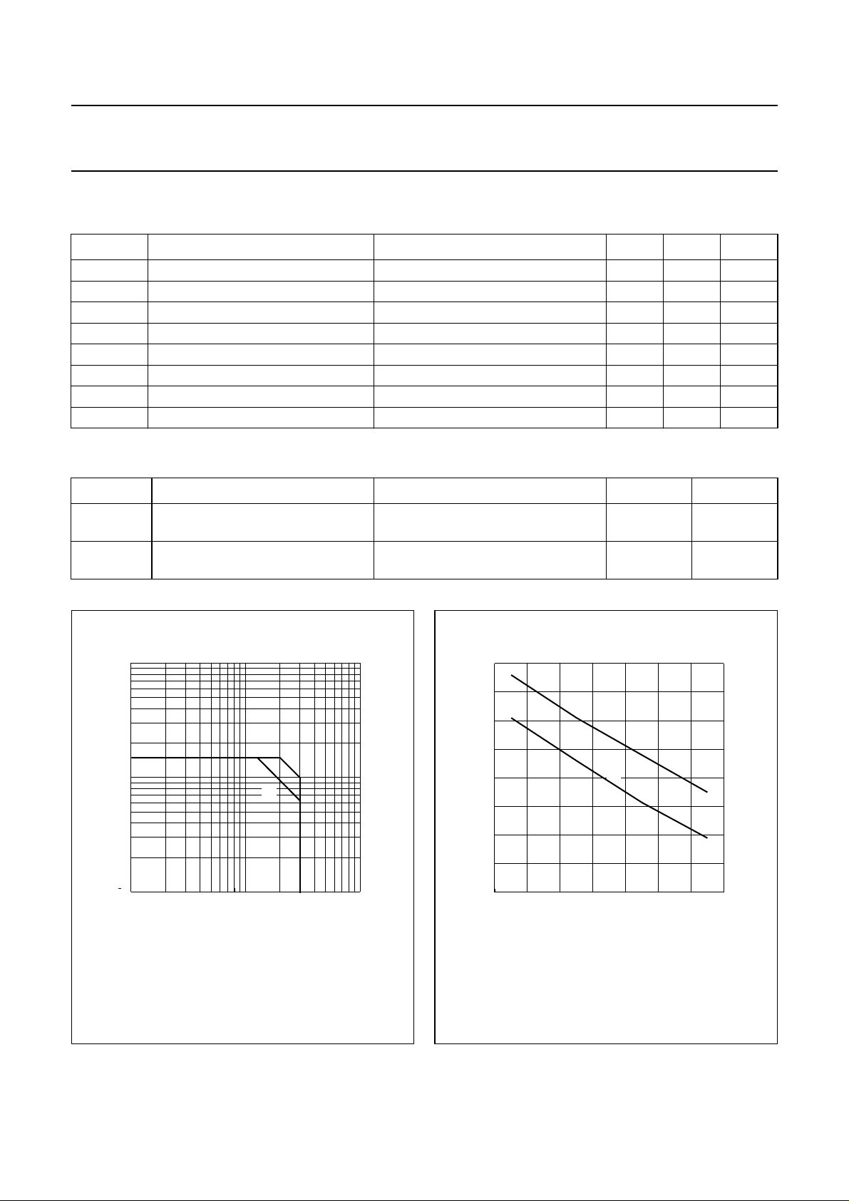
10
handbook, halfpage
I
C
(A)
1
1
10
11010
(1) Tmb=25°C.
(2) Th=70°C.
(2)
Fig.2 DC SOAR.
(1)
VCE(V)
MLC658
handbook, halfpage
2
40
P
tot
(W)
30
20
10
0
0 20 40 60 80 100 120 140
(1) Continuous operation.
(2) Short-time operation during mismatch.
(2)
(1)
MLC659
o
T ( C)
h
Fig.3 Power derating curves.
1995 Apr 11 3
Philips Semiconductors Product specification
UHF power transistor BLV910
CHARACTERISTICS
T
=25°C unless otherwise specified.
j
SYMBOL PARAMETER CONDITIONS MIN. TYP. MAX. UNIT
V
(BR)CBO
V
(BR)CEO
V
(BR)EBO
I
CES
h
FE
C
c
C
re
collector-base breakdown
voltage
collector-emitter breakdown
voltage
emitter-base breakdown
voltage
collector leakage current VBE= 0; VCE=28V −−0.75 mA
DC current gain VCE= 10 V; IC= 0.5 A; 30 − 120
collector capacitance VCB= 26 V; IE=ie= 0; f = 1 MHz − 10 − pF
feedback capacitance VCE= 26 V; IC= 0; f = 1 MHz − 6 − pF
open emitter; IC= 5 mA 70 −−V
open base; IC=15mA 30 −−V
open collector; IE= 0.3 mA 3 −−V
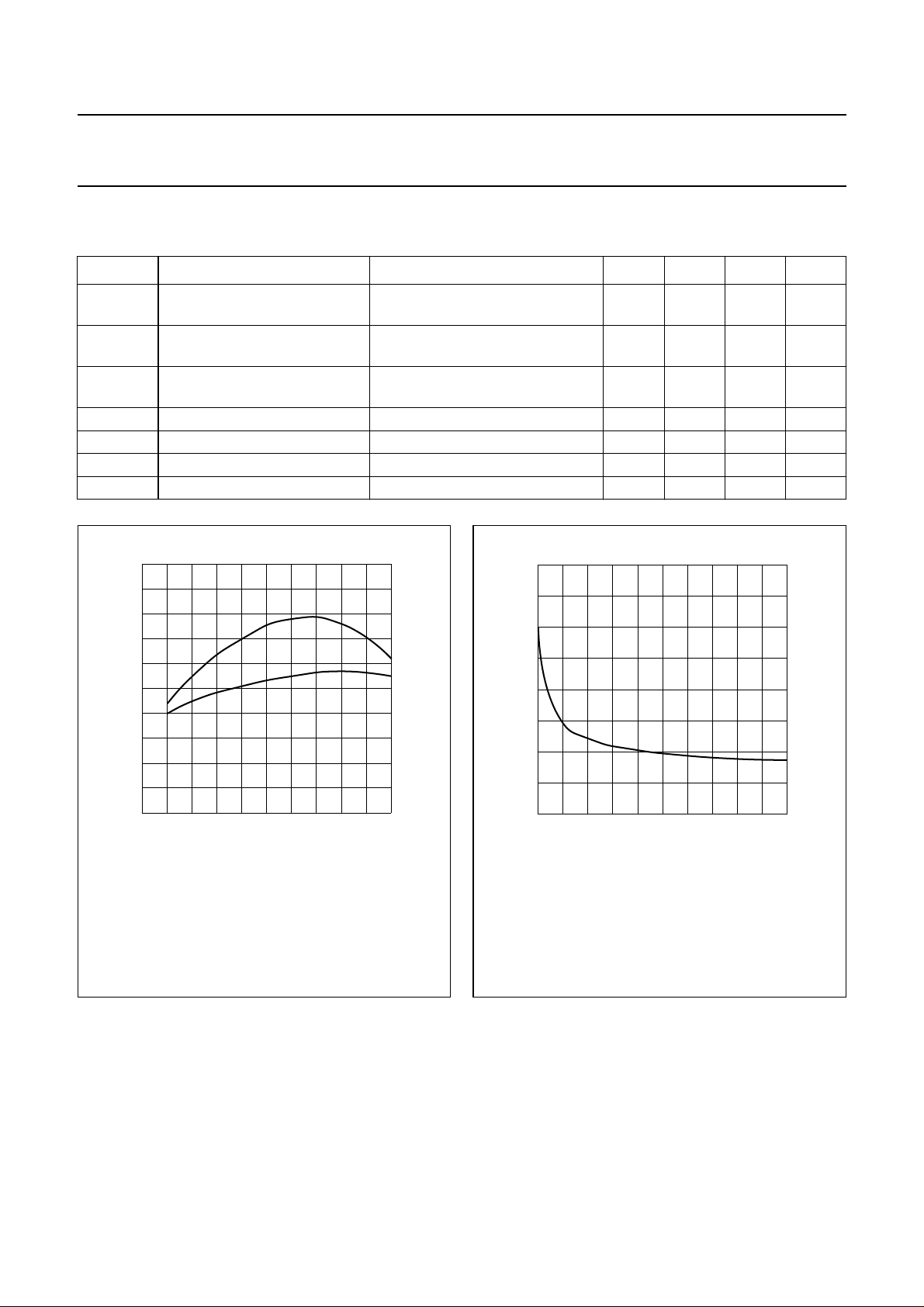
100
handbook, halfpage
h
FE
80
60
40
20
0
0 0.5 1.0 1.5 2.0 2.5
(1) VCE= 26 V: measured under pulsed conditions;
≤ 500 µs; δ<0.01.
t
p
(2) VCE=10V.
(1)
(2)
Fig.4 DC current gainas a function of collector
current; typical values.
MLC660
IC(A)
40
handbook, halfpage
C
c
(pF)
30
20
10
0
01020304050
IE=ie= 0; f = 1 MHz.
Fig.5 Collector capacitance as a function of
collector-base voltage; typical values.
MLC661
VCB(V)
1995 Apr 11 4
 Loading...