

Philips BLV909 Datasheet
DISCRETE SEMICONDUCTORS
DATA SH EET
M3D175
BLV909
UHF power transistor
Product specification
Supersedes data of 1996 Nov 04
1999 Jun 25
Philips Semiconductors Product specification
UHF power transistor BLV909
FEATURES
• Emitter ballasting resistors for optimum temperature
profile
• Gold metallization ensures excellent reliability
• Internal input matching to achieve high power gain and
easy design of wideband circuits.
APPLICATIONS
• Common emitter class-AB operation in base stations in
the 820 to 960 MHz frequency range.
DESCRIPTION
NPN silicon planar epitaxial transistor in an 8-lead
SOT409B SMD package with a ceramic cap. All leads are
isolated from the mounting base.
QUICK REFERENCE DATA
RF performance at T
=25°C in a common emitter test circuit.
mb
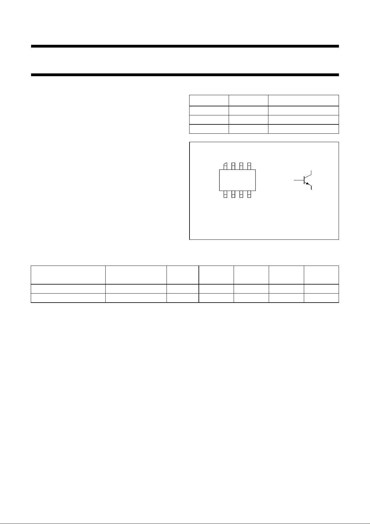
PINNING - SOT409B
PIN SYMBOL DESCRIPTION
1, 4, 5, 8 e emitter
2, 3 b base
6, 7 c collector
handbook, halfpage
85
14
Top view
MSA467
Fig.1 Simplified outline and symbol.
c
b
e
MODE OF OPERATION
f
(MHz)
V
(V)
CE
P
(W)
L
G
(dB)
p
η
C
(%)
CW, class-AB 960 26 9 ≥9.5 ≥50 −
2-tone, class-AB f1= 960; f2= 960.1 26 9 (PEP) ≥9.5 ≥35 typ. −30
d
im
(dBc)
1999 Jun 25 2
Philips Semiconductors Product specification
UHF power transistor BLV909
LIMITING VALUES
In accordance with the Absolute Maximum Rating System (IEC 134).
SYMBOL PARAMETER CONDITIONS MIN. MAX. UNIT
V
CBO
V
CEO
V
EBO
I
C
I
C(AV)
P
tot
T
stg
T
j
THERMAL CHARACTERISTICS
SYMBOL PARAMETER CONDITIONS VALUE UNIT
R
th j-mb
collector-base voltage open emitter − 70 V
collector-emitter voltage open base − 30 V
emitter-base voltage open collector − 3V
collector current (DC) − 1.5 A
average collector current − 1.5 A
total power dissipation Tmb=25°C; note 1 − 29 W
storage temperature −65 +150 °C
operating junction temperature − 200 °C
thermal resistance from junction to
P
= 29 W; Tmb=25°C; note 1 6 K/W
tot
mounting base
Note to the Limiting values and Thermal characteristics
1. Transistor with metallized ground plane mounted on a printed-circuit board, see
Handbook SC19a.”
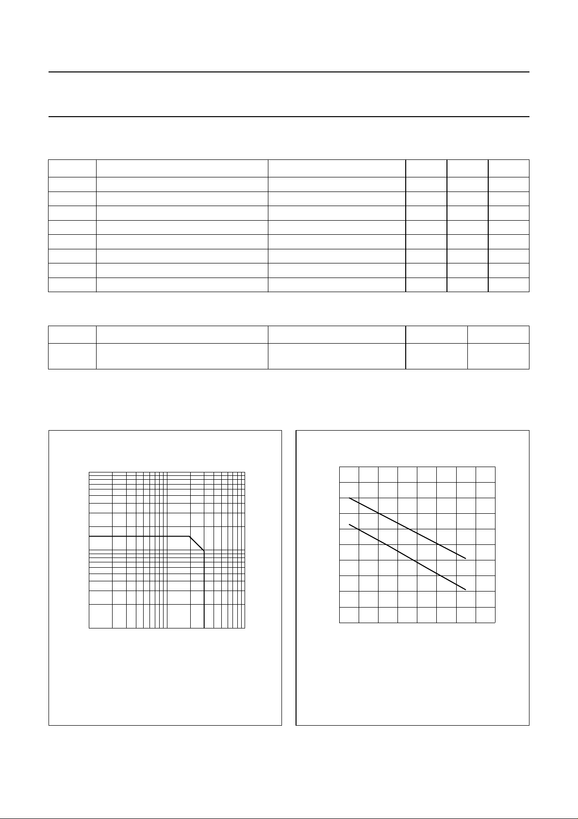
10
handbook, halfpage
I
C
(A)
1
−1
10
11010
VCE (V)
MGG301
2
50
handbook, halfpage
P
tot
(W)
40
30
20
10
0
040
“Mounting and soldering section,
MGD273
(1)
(2)
80 160
120
Tmb (
o
C)
Tmb=25°C.
Fig.2 DC SOAR.
1999 Jun 25 3
(1) Short-time operation during mismatch.
(2) Continuous operation.
Fig.3 Power derating curves.

Philips Semiconductors Product specification
UHF power transistor BLV909
CHARACTERISTICS
=25°C unless otherwise specified.
T
j
SYMBOL PARAMETER CONDITIONS MIN. TYP. MAX. UNIT
V
(BR)CBO
V
(BR)CEO
V
(BR)EBO
I
CES
h
FE
C
c
C
re
collector-base breakdown voltage open emitter; IC=5mA 70 −−V
collector-emitter breakdown voltage open base; IC=15mA 30 −−V
emitter-base breakdown voltage open collector; IE= 0.3 mA 3 −−V
collector leakage current VCE= 28 V; VBE=0 −−0.75 mA
DC current gain VCE= 10 V; IC= 500 mA 30 − 120
collector capacitance VCB= 26 V; IE=ie= 0; f = 1 MHz − 10 − pF
feedback capacitance VCE= 26 V; IC= 0; f = 1 MHz − 6 − pF
100
handbook, halfpage
h
FE
80
60
40
20
0
012
(1) VCE= 26V; tp= 500 µs; δ≤1%.
(2) VCE=10V.
(1)
(2)
MGD274
I
(A)
C
Fig.4 DC current gain as a function of collector
current; typical values.
60
handbook, halfpage
C
(pF)
40
20
C
c
C
3
0
f = 1 MHz.
10 50
0
re
20 30 40
MGG302
VCB (V)
Fig.5 Collector and feedback capacitance as a
function of collector-base voltage; typical
values.
1999 Jun 25 4
Philips Semiconductors Product specification
UHF power transistor BLV909
APPLICATION INFORMATION
RF performance at T
=25°C in a common emitter test circuit (see Figs 12 and 13).
mb
MODE OF OPERATION
f
(MHz)
V
(V)
CE
I
CQ
(mA)
P
(W)
L
G
p
(dB)
η
(%)
C
d
im
(dBc)
CW, class-AB 960 26 25 9 ≥9.5, typ. 11.5 ≥50, typ. 55 −
2-tone, class-AB f1= 960; f2= 960.1 26 25 9 (PEP) ≥9.5, typ. 11.5 ≥35, typ. 40 typ. −30
Ruggedness in class-AB operation
The BLV909 is capable of withstanding a load mismatch corresponding to VSWR = 20 : 1 through all phases under the
following conditions: f = 960 MHz; V
16
handbook, halfpage
G
p
(dB)
12
8
4
G
p
η
C
= 26 V; ICQ= 25 mA; Tmb=25°C.
CE
MGG304
80
η
(%)
60
40
20
C
handbook, halfpage
P
(W)
16
L
12
8
4
MGG303
0
04812
VCE= 26 V; ICQ= 25 mA; f = 960 MHz.
PL (W)
Fig.6 Power gain and collector efficiency as
functions of load power; typical values.
0
0
0
VCE= 26 V; ICQ= 25 mA; f = 960 MHz.
0.4 1.6
0.8 1.2
PD (W)
Fig.7 Load power as a function of drive power;
typical values.
1999 Jun 25 5
 Loading...