

Philips BLV897 Datasheet

DISCRETE SEMICONDUCTORS
DATA SH EET
BLV897
UHF push-pull power transistor
Preliminary specification
Supersedes data of 1997 Oct 03
1997 Nov 10
Philips Semiconductors Preliminary specification
UHF push-pull power transistor BLV897
FEATURES
• Internal input matching for an optimum wideband
capability and high gain
• Polysilicon emitter ballasting resistors for an optimum
temperature profile
• Gold metallization ensures excellent reliability.
APPLICATIONS
• Common emitter class-AB operation in base stations in
the 800 to 960 MHz frequency band.
DESCRIPTION
NPN silicon planar transistor with two sections in push-pull
configuration. The device is encapsulated in a SOT324B
4-lead rectangular flange package with a ceramic cap.
The common emitters are connected to the flange.
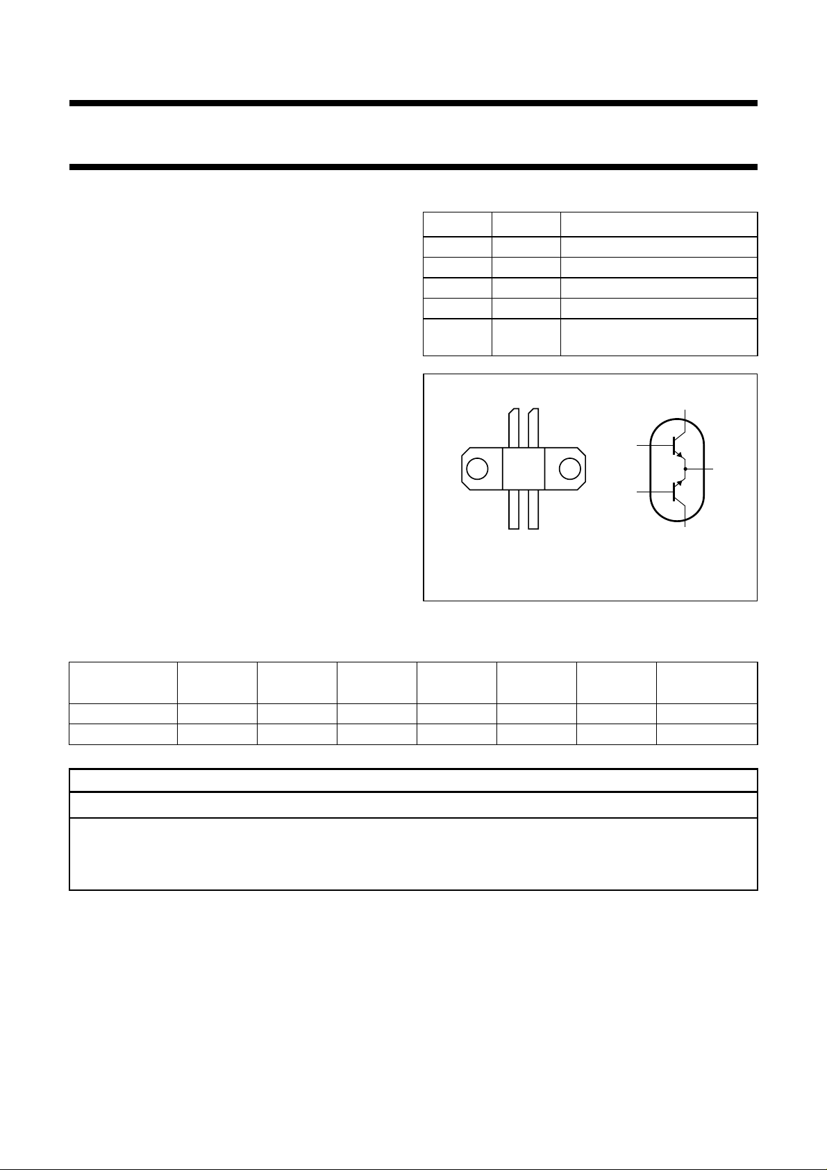
PINNING - SOT324B
PIN SYMBOL DESCRIPTION
1 c1 collector 1
2 c2 collector 2
3 b1 base 1
4 b2 base 2
5 e common emitters connected to
flange
handbook, halfpage
12
b1
Top view
3
5
4
b2
MAM217
Fig.1 Simplified outline and symbol.
c1
e
c2
QUICK REFERENCE DATA
RF performance at T
MODE OF
OPERATION
=25°C in a common emitter push-pull test circuit.
h
f
(MHz)
V
(V)
CE
I
CQ
(mA)
P
(W)
L
G
(dB)
p
η
C
(%)
d
3
(dBc)
CW, class-AB 900 24 2 × 80 30 ≥10 ≥45 −
2-tone, class-AB 900 24 2 × 80 30 (PEP) ≥11 ≥35 <−32; typ. −37
WARNING
Product and environmental safety - toxic materials
This product contains beryllium oxide. The product is entirely safe provided that the BeO discs are not damaged.
All persons who handle, use or dispose of this product should be aware of its nature and of the necessary safety
precautions. After use, dispose of as chemical or special waste according to the regulations applying at the location of
the user. It must never be thrown out with the general or domestic waste.
1997 Nov 10 2

Philips Semiconductors Preliminary specification
UHF push-pull power transistor BLV897
LIMITING VALUES
In accordance with the Absolute Maximum Rating System (IEC 134).
SYMBOL PARAMETER CONDITIONS MIN. MAX. UNIT
V
CBO
V
CEO
V
EBO
I
C
I
C(AV)
P
tot
T
stg
T
j
Note
1. Total device; both sections equally loaded.
collector-base voltage open emitter − 70 V
collector-emitter voltage open base − 30 V
emitter-base voltage open collector − 3V
collector current (DC) − 5A
average collector current − 5A
total power dissipation Tmb=25°C; note 1 − 97 W
storage temperature −65 +150 °C
operating junction temperature − 200 °C
THERMAL CHARACTERISTICS
SYMBOL PARAMETER CONDITIONS VALUE UNIT
R
th j-mb
R
th mb-h
thermal resistance from junction to mounting base P
= 97 W; note 1 1.79 K/W
tot
thermal resistance from mounting base to heatsink note 1 0.4 K/W
Note
1. Total device; both sections equally loaded.
CHARACTERISTICS
Values apply to either transistor section; T
=25°C unless otherwise specified.
j
SYMBOL PARAMETER CONDITIONS MIN. TYP. MAX. UNIT
V
(BR)CBO
V
(BR)CEO
V
(BR)EBO
I
CBO
h
FE
C
c
collector-base breakdown voltage IC= 15 mA; IE=0 70 −−V
collector-emitter breakdown voltage IC= 30 mA; IB=0 30 −−V
emitter-base breakdown voltage IE= 0.6 mA; IC=0 3 −−V
collector-base leakage current VCB= 28 V; VBE=0 −−1.5 mA
DC current gain VCE= 10 V; IC=1A 30 − 120
collector capacitance VCB= 24 V; IE=ie= 0; f = 1 MHz − 18 − pF
1997 Nov 10 3

Philips Semiconductors Preliminary specification
UHF push-pull power transistor BLV897
APPLICATION INFORMATION
RF performance at T
=25°C in a common emitter push-pull class-AB test circuit.
h
MODE OF
OPERATION
f
(MHz)
V
(V)
CE
I
CQ
(mA)
P
(W)
L
G
p
(dB)
η
(%)
C
d
3
(dBc)
CW, class-AB 900 24 2 × 80 30 ≥10 ≥45 −
2-tone, class-AB 900 24 2 × 80 30 (PEP) ≥11 ≥35 <−32; typ. −37
Ruggedness in class-AB operation
The BLV897 is capable of withstanding a load mismatch corresponding to VSWR =5:1 through all phases under the
conditions: V
= 24 V; ICQ=2×80 mA; f = 900 MHz; Th=25°C; PL= 30 W. The transistor is also capable of
CE
withstanding a load mismatch corresponding to VSWR = 10 : 1 through all phases at PL= 30 W (PEP).
50
handbook, halfpage
P
L
(W)
40
30
20
10
MBK287
14
handbook, halfpage
G
p
(dB)
12
10
8
6
4
2
G
p
η
C
MBK286
70
η
C
(%)
60
50
40
30
20
10
0
012 65
VCE= 24V; ICQ=2×80 mA; f= 900 MHz.
4
3
PD (W)
Fig.2 Load power as a function of drive power;
typical values.
1997 Nov 10 4
0
01020
VCE= 24 V; ICQ=2×80 mA; f = 900 MHz.
30
40 50
PL (W)
Fig.3 Power gain and collector efficiency as
functions of load power; typical values.
0
 Loading...